Back to Home
Squelch IC
Detailed Information
By Robert W. Meister WA1MIK

|
Back to MICOR index Back to Home |
Motorola M6709 Squelch IC Detailed Information By Robert W. Meister WA1MIK |
|
Background:
Kevin Custer W3KKC sent me one of his Squelch CTCSS kits (SC-50) minus the squelch chip, since I had a MICOR station audio/squelch board here that I could take the chip out of. Click here to go to the SC-50 web page. I assembled the unit; the PL circuit worked fine but the squelch circuit refused to close, so the blue LED was always lit. In an effort to discover why, I took detailed AC and DC voltage measurements using a 10 kHz signal to simulate noise going into the chip. The filter sections were working fine; I determined the detector or switching logic sections of the chip were defective. Kevin sent me another M6709 and the board now works fine. I repeated the measurements on a properly functioning chip and tabulated them below.
I usually refer to the squelch chip as the M6709. It also goes by newer part numbers M7716 and SC7716. These are all the same part.
Since there's no data sheet for these chips, all we can do is reverse-engineer it and determine how it works by feeding signals into it and looking at the outputs.
Measurement Conditions:
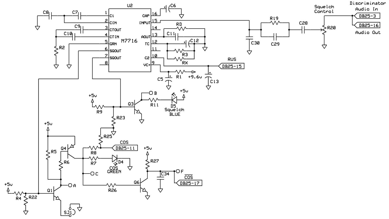
Testing was done with the M6709 installed in Kevin's SC-50 board. A 10 kHz sine wave tone at 70mVAC was injected into the input of the board. The squelch pot was set fully clockwise. Jumper SJ2 installed. All readings were taken with a Fluke model 189 true RMS digital multi-meter. Resistances were taken with the M6709 removed from its socket. A partial schematic of the SC-50 board is shown below. Click on it for a larger image.
M6709 Squelch Chip Voltage Readings:
| M6709 | Book | Book | M6709 on SC-50 Board | Ohms | ||||
|---|---|---|---|---|---|---|---|---|
| IC Pin | SQ | UNSQ | 10 kHz SQ | No Sig UNSQ | To | |||
| # | Function | VDC | VDC | VDC | mVAC | VDC | mVAC | Gnd |
| 1 | 1st Amp Out | 4.1 | 4.1 | 4.51 | 374 | 4.52 | 0 | Inf |
| 2 | 2nd Amp In | 2.2 | 2.2 | 2.15 | 188 | 2.15 | 0 | Inf |
| 3 | 2nd Amp Out | 4.0 | 4.0 | 4.30 | 1395 | 4.26 | 7 | Inf |
| 4 | Detector In | 1.6 | 0.9 | 1.68 | 566 | 0.98 | 7 | Inf |
| 5 | Ground | 0.0 | 0.0 | 0.00 | 0 | 0.00 | 0 | Inf |
| 6 | Shunt Switch Out | 0.02 | 0 | 2.45 | 0 | 2.8k | ||
| 7 | Shunt Switch Out | 0.02 | 0 | 0.69 | 0 | 2.8k | ||
| 8 | PL Decoder In | 0.00 | 3 | 0.00 | 3 | Inf | ||
| 9 | Vcc In | 9.4 | 9.4 | 9.52 | 1 | 9.53 | 0 | 2M |
| 10 | Rx Unsq Ind Out | 6-9 | 0.0 | 8.49 | 0 | 0.20 | 0 | Inf |
| 11 | Mute In | 0.13 | 330 | 0.04 | 284 | Inf | ||
| 12 | Short/Long Tail | 0.00 | 0 | 0.00 | 0 | 181k | ||
| 13 | Ch Act Ind Out | 1.1 | 6.3 | 1.06 | 26 | 6.47 | 0 | Inf |
| 14 | Sq Disable In | 0.00 | 3 | 9.51 | 2 | Inf | ||
| 15 | 1st Amp In | 2.2 | 2.2 | 2.18 | 30 | 0.01 | 0 | Inf |
| 16 | 6.4V Filter Cap | 6.4 | 6.4 | 6.69 | 3 | 6.69 | 0 | Inf |
Note: the unsquelched DC voltage on pin 6 will be the same as pin 7 if jumper SJ1 is installed rather than jumper SJ2.
M6709 Filter Response:
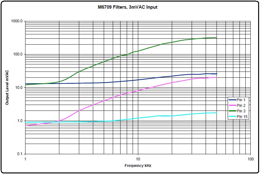
Since I now had a working MICOR squelch circuit on the bench, I wondered what the filters - composed of the 1st and 2nd amplifier stages - were doing. The noise from the radio's discriminator or detector output (or in this case a sine wave generated by an HP 339A distortion analyzer) reaches pin 15 through the squelch pot and a small high-pass filter. The 1st amplifier boosts that signal by about 15. Another high-pass filter sends that signal to the input of the 2nd amplifier, which also boosts its signal by about 15. These two stages will go into limiting when a large-enough signal is present. I purposely used a very low input signal level to prevent limiting, thus the graph below shows the actual filter frequency response. You'll notice that the input and output signals for each amplifier (pins 15 and 1, pins 2 and 3) are identical except for the higher amplitude due to the gain. Click on the image for a larger view.
M6709 Squelch Threshold:
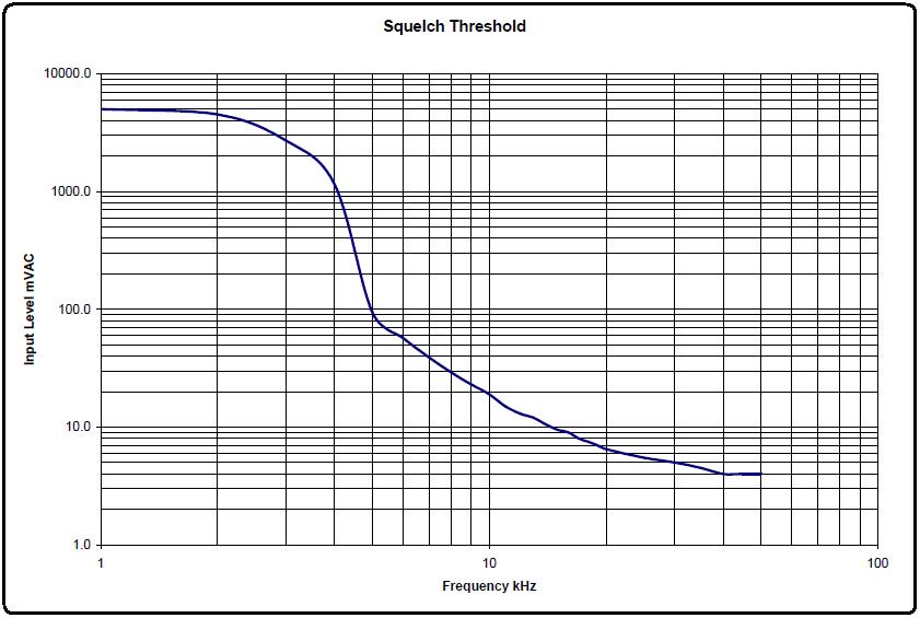
Noise squelch systems must ignore signals in the voice frequency range of about 300 to 3400 Hz. The MICOR squelch is no exception. All of the high-pass filtering is designed to eliminate any voice energy and only look at the noise energy above about 5 kHz. I fed a signal into the SC-50 with the squelch pot set fully clockwise (maximum sensitivity) and noted the level that caused the blue LED to turn off (close squelch). Remember, with no input signal, the M6709 considers this a full-quieting signal and the squelch will be open, allowing the blue LED to turn on. As the noise (or high-frequency input signal) increases, the M6709 detects this and closes the squelch, turning off the blue LED. When the squelch is closed, the two shunt switch pins on the M6709 impose a very low resistance to ground, which is used to mute the received audio. In the SC-50, this shunts the base drive to Q3, disabling the blue LED and indicating a closed squelch. I just fed in enough signal from an HP 339A distortion analyzer at various frequencies to cause the blue LED to turn off and recorded the level needed to do that. The graph below shows that the M6709 is relatively insensitive to signals below about 4 kHz, but it becomes quite sensitive to signals above about 5 kHz, eventually reaching its limit at 50 kHz. Since squelch noise is in the 5-30 kHz range, you can see that this is the band where the M6709 is most responsive. Click on the image for a larger view.
M6709 Squelch Tail Response:
I connected the SC-50 to a detected audio signal on an 800 MHz Motorola MaxTrac mobile radio (it was the first one I grabbed). This is equivalent to the Flat RX Audio output on the 16-pin accessory jack, but since this radio only had a 5-pin accessory jack, I had to utilize the point labeled "RXA" on the logic board. I isolated the radio with a 10uF capacitor to remove the DC voltage present on this point. There was plenty of signal level available here, in fact too much for the SC-50, so I added a 100k resistor in series with the SC-50's input pin. I set the squelch pot at threshold so the blue LED went off and stayed off. I connected an Agilent E4430B RF signal generator to the radio's antenna jack and fed in an un-modulated RF signal. I monitored the headset audio output of the radio, as this is de-emphasized and at a fixed level. I also monitored the DC voltage on pin 13 of the M6709. I graphed the results, shown below. The X-axis is the RF Input Level. The Y-axis on the left is the dB Quieting. Click on the graph for a larger image.
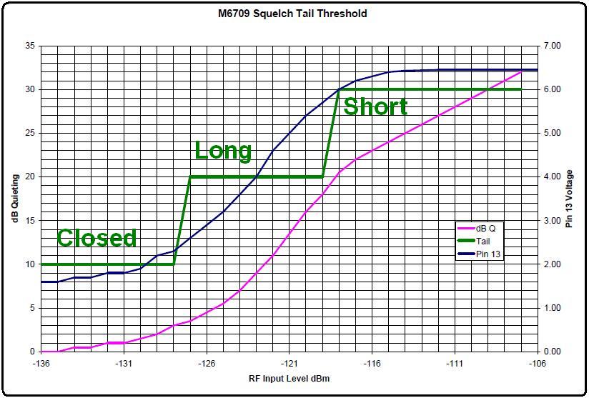
In this graph, the purple trace is the dB quieting level; of significance is the 20dB point, which was reached at -118dBm. The green trace depicts the squelch action: the squelch was closed until the input signal level reached -127dBm, at which point the blue LED turned on, indicating the squelch had opened. The squelch tail was long at this point, but it became short when the input signal level reached -118dBm, which coincides with the 20dB quieting point. The blue trace depicts the voltage on pin 13 of the M6709 and the scale for that is on the right side of the graph. The M6709 decides when to change from long to short squelch tail based on this voltage.
M6709 Schematic:
Based on usage in radio squelch circuits and on the SC-50 squelch board, I have assigned pin numbers in red to the schematic of the M6709 found in the patent information. I suspect that the actual manufactured ICs are slightly different from the patent. I have added external parts values in green based on several mobile and station schematics. Click on the image below for a much larger version.
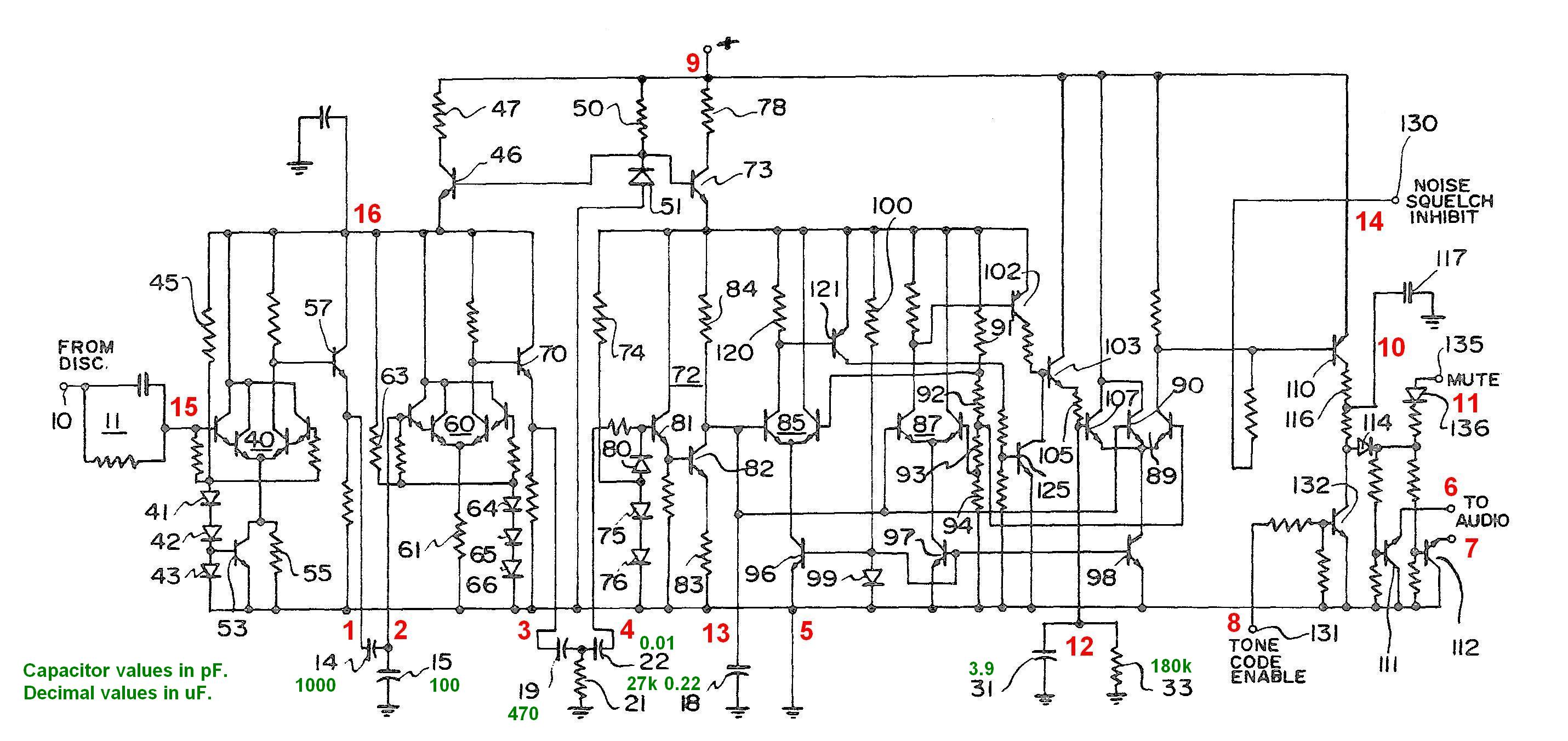
M6709 Pin Descriptions:
| Pin | Description, Function, Use, Attached Components |
|---|---|
| 1 | 1st Amplifier Output. Connects to pin 2 through a capacitor, nominally 1000pF. This is the first stage high-pass filter. |
| 2 | 2nd Amplifier Input. Connects to pin 1 through a capacitor. Also has a capacitor to ground, nominally 100pF. |
| 3 | 2nd Amplifier Output. Connects to pin 4 through two capacitors, 470pF and 0.01uF with a resistor to ground at the junction, typically 27k. This is the second stage high-pass filter. |
| 4 | Detector Input. Connects to pin 3 through a capacitor. |
| 5 | Ground |
| 6 | Shunt Switch output, emitter. Conducts to ground to mute the audio path and is usually AC-coupled. Don't supply more than about +4VDC to this pin. |
| 7 | Shunt Switch output, emitter. Conducts to ground to mute the audio path and is usually AC-coupled. Don't supply more than about +4VDC to this pin. |
| 8 | PL Decoder input. It is pulled low internally. When pulled high, it removes the turn-on drive from the two shunt switches, rendering them high-Z, un-muting the audio path. You could pull this input high with an external PL decoder to open the squelch, or as an over-ride to open the squelch when pushed, like a MON pushbutton. |
| 9 | +Vcc, normally +9.6VDC |
| 10 | Receiver Un-squelched Indicator. Is pulled high by the IC when the two shunt switches are turned on, rendering them low-Z, muting the audio path. Has a 2.2uF capacitor to ground. |
| 11 | Mute input. When pulled high, it causes the two shunt switches to turn on, rendering them low-Z, muting the audio path. This would be done in a mobile rig to mute the receiver when transmitting. |
| 12 | Short/Long Squelch Threshold. Usually has a 3.3uF capacitor and a 180k resistor to ground. These components select the duration of the long squelch tail. |
| 13 | Channel Activity Indicator. Usually has a 0.22uF capacitor to ground. |
| 14 | Noise Squelch Inhibit input. When pulled low, it applies drive to the two shunt switches to turn them on, rendering them low-Z, muting the audio path, similar to applying a high to pin 11. Pin 8 high will over-ride pin 14 low. This defeats the noise squelch circuit, keeping the audio path muted unless a PL signal is present. This pin was grounded in the early PL radios because Motorola figured the reverse-burst would completely eliminate the need for any sort of noise squelch. |
| 15 | 1st Amplifier Input. The discriminator audio signal from the receiver is fed to a squelch pot, which feeds this pin through a parallel RC network consisting of a 750pF capacitor and a 22k resistor. There's also a 100pF capacitor on this pin to ground. The nominal input to this pin is 15 millivolts RMS. |
| 16 | 6.4V Regulator filter capacitor, nominally 4.7uF. |
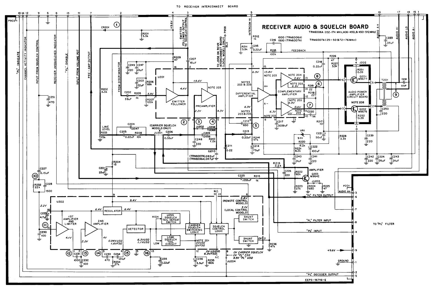
A typical circuit schematic from a Motorola MICOR station audio/squelch board is shown below; the mobile board is slightly different. U202 in the lower left section is the M6709 chip. The thick black lines show the audio path. Note that the shunt switch output, pin 7, shunts the audio signal to mute the receiver audio. In mobile audio/squelch boards, the second shunt switch output, pin 6, is also used to mute the receiver audio. Click on the image for a larger view.
Acknowledgements and Credits:
The schematic of the M6709 IC came from US patent # 3,628,058: "Integrated Dual Time Constant Squelch Circuit" patented by Roy H. Espe on December 14, 1971.
Radio schematics came from Motorola MICOR manuals.
The SC-50 partial schematic was taken from Kevin's excellent SC-50 documentation.
Contact Information:
The author can be contacted at: his-callsign [ at ] comcast [ dot ] net.
This page was created 10-Mar-2015
Go to the top of this page
Back to the MICOR index
Back to the Home page
Article text © Copyright 2015 and date of last update by Robert W. Meister WA1MIK.
This web page, this web site, the information presented in and on its pages and in these modifications and conversions is © Copyrighted 2007 and (date of last update) by Kevin Custer W3KKC and multiple originating authors. All Rights Reserved, including that of paper and web publication elsewhere.