Motorola index
Back to Home
Into a CLB Station
By Robert W. Meister WA1MIK

|
MSF index Motorola index Back to Home |
Installing a CXB SSCB Into a CLB Station By Robert W. Meister WA1MIK |
|
Enough people have asked the question and either not looked for, or not been able to find, the answer. I figured it was about time for a real article about it.
CLB and CXB refer to the three letters in the station's model number. These are generic letters that specify an analog station (CLB) or a digital-capable station (CXB).
This procedure should be possible on any MSF5000 station, except that the control boards used on 896 MHz stations have additional circuitry on them to support the HearClear noise-reduction system. The 896 MHz stations have GFB in the model number and are called Analog-Plus. These still use RSS for programming but can't have secure encryption added; that's only possible with digital-capable (CXB) stations on 800 MHz and below. The SSCB board is different for this application. It is not known if an 896 MHz analog station can utilize an SSCB built for non-896 MHz use.
Click on any of the images or photos for larger views. Some of them are 300kb.
Background:
CLB stations require EPROMs (Erasable Programmable Read-Only Memory) and suitcase programmers to change any operating parameters. Not everyone has access to the equipment to do this, so they acquire CXB SSCB (Secure-capable Station Control Board) boards and try to install them in their CLB stations. Physically, the boards slip right in to the control tray and plug in with the existing cables, but the stations do not work after that. The primary reason is that on CLB stations, the SCB (Station Control Board) provides a source of +5V which is fed down the flat cable to the interconnect board underneath the RF tray. It is then distributed to the Uniboard in the RF tray to power the TTL logic in the transmit and receive synthesizers. (Everything else in the RF tray operates on 9.6V or A+.) The current drain is only about 100 mA, certainly just a drop in the bucket compared to the other 5V logic on the SCB. The +5V supply signal is fed from the SCB to the interconnect board via J801 pin 9.
In the CXB stations, the interconnect board under the RF tray has a three-terminal 5V regulator on it to supply the Uniboard in the RF tray. It gets its input power (+9.6V) from the IPA board in the RF tray. Thus, there's no need for +5V to come from the SSCB, and in fact Motorola used that signal line in the flat cable to support a second receiver in some configurations. It's likely that the second receiver requirement came first, then they added a 5V regulator on the interconnect board to free up that wire in the control cable. J801 pin 9 is labeled "RX2 Strobe".
When the CXB SSCB is installed in the CLB station, +5V is not provided to the interconnect board or the Uniboard, so the station doesn't function. The VCOs don't lock and multiple errors, all related to the VCOs or synthesizers, are displayed. It's actually very easy to fix.
SCB and SSCB Radio Interface (J801) Connector Signals:
Pins with green background are the same in both the analog (SCB) and digital-capable (SSCB) control units.
Pins with orange backgrounds are grounded in the analog (SCB) units but provide support for a second receiver in the digital-capable (SSCB) units.
Pins with red background are different and require modification to the SSCB if it is to be installed into an analog station (that had an SCB).
(In) or (Out) in a signal name indicates the direction IN to or OUT of the SCB/SSCB.
An asterisk after a signal name means it is active low.
| Pin | SCB Usage | SSCB Usage |
|---|---|---|
| 1 | +9.6V (In) | +9.6V (In) |
| 2 | Audio Ground | RX2 VCO Lock (In) * |
| 3 | TX Mod Audio (Out) | TX Mod Audio (Out) |
| 4 | Audio Ground | Audio Ground |
| 5 | RX Audio (In) | Raw RX1 Audio (In) |
| 6 | Audio Ground | Raw RX2 Audio (In) |
| 7 | Antenna Relay (Out) * | Antenna Relay (Out) * |
| 8 | TX VCO Lock (In) * | TX VCO Lock (In) * |
| 9 | +5V (Out) | RX2 Strobe (Out) |
| 10 | PA Full Power (In) * | PA Full Power (In) * |
| 11 | Logic Ground | AGC Reference (In) |
| 12 | PA On (In) * | PA On (In) * |
| 13 | RX Loop (In) | RX1 Loop (In) |
| 14 | PA Key (Out) * | PA Key (Out) * |
| 15 | RX VCO Lock (In) * | RX1 VCO Lock (In) * |
| 16 | PA Power Cutback * | PA Power Cutback * |
| 17 | SD0 | SD0 |
| 18 | TX Loop (In) | TX Loop (In) |
| 19 | SD1 | SD1 |
| 20 | SA2 | SA2 |
| 21 | SD2 | SD2 |
| 22 | SA1 | SA1 |
| 23 | SD3 | SD3 |
| 24 | SA0 | SA0 |
| 25 | RX Strobe (Out) | RX1 Strobe (Out) |
| 26 | TX Strobe (Out) | TX Strobe (Out) |
Adding +5V:
You can add your own three-terminal regulator (and support components) to the interconnect board, if you have the schematic and are willing to take the time to disassemble the station enough to get the interconnect board out and work on it. Motorola supplied a kit that either had a new interconnect board, or a separate circuit board with a three-terminal regulator on it that was wired to the CLB interconnect board. I've never seen one.
You can add a wire to the solder-side of the SSCB to route +5V to J801 pin 9. This can be accomplished several ways; one method is described here. This depends on the parts layout of your SSCB, but it was quite easy to follow the traces and identify the parts once I saw the schematic. The photo below shows the components around Q811.
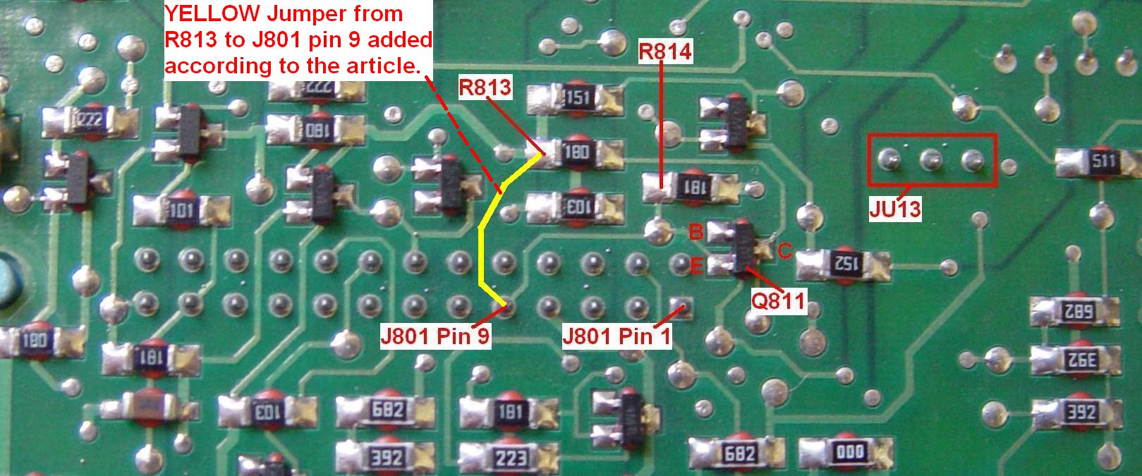
The schematic diagram for these parts is shown below. You can see that the emitter lead of Q811 goes directly to J801 pin 9. You can run a short piece of wire from +5V, which can be found at the wider foil on the left (labeled) side of R813 (18 ohm resistor marked "180") that runs to the collector lead of Q811, to the emitter lead of Q811 that has R814 attached to it (180 ohm resistor marked "181"), or directly to J801 pin 9. You can run the wire to any of the solder pads that will make the connection. One such method is shown on the photo with a yellow line. Your board may be laid out slightly different, so follow the traces and component values.
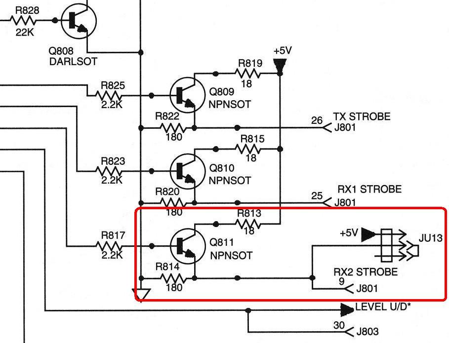
On those SSCB boards so equipped, you can simply move jumper JU13 from its "Normal" position to its "Alternate" position. It seems that this modification was necessary often enough that Motorola engineered it into their boards and documented it. Perhaps there are other uses for the SSCB in equipment that doesn't have an external source of +5V. Note that this performs the same function as adding the wire around Q811. Refer to the schematic above.
Documentation:
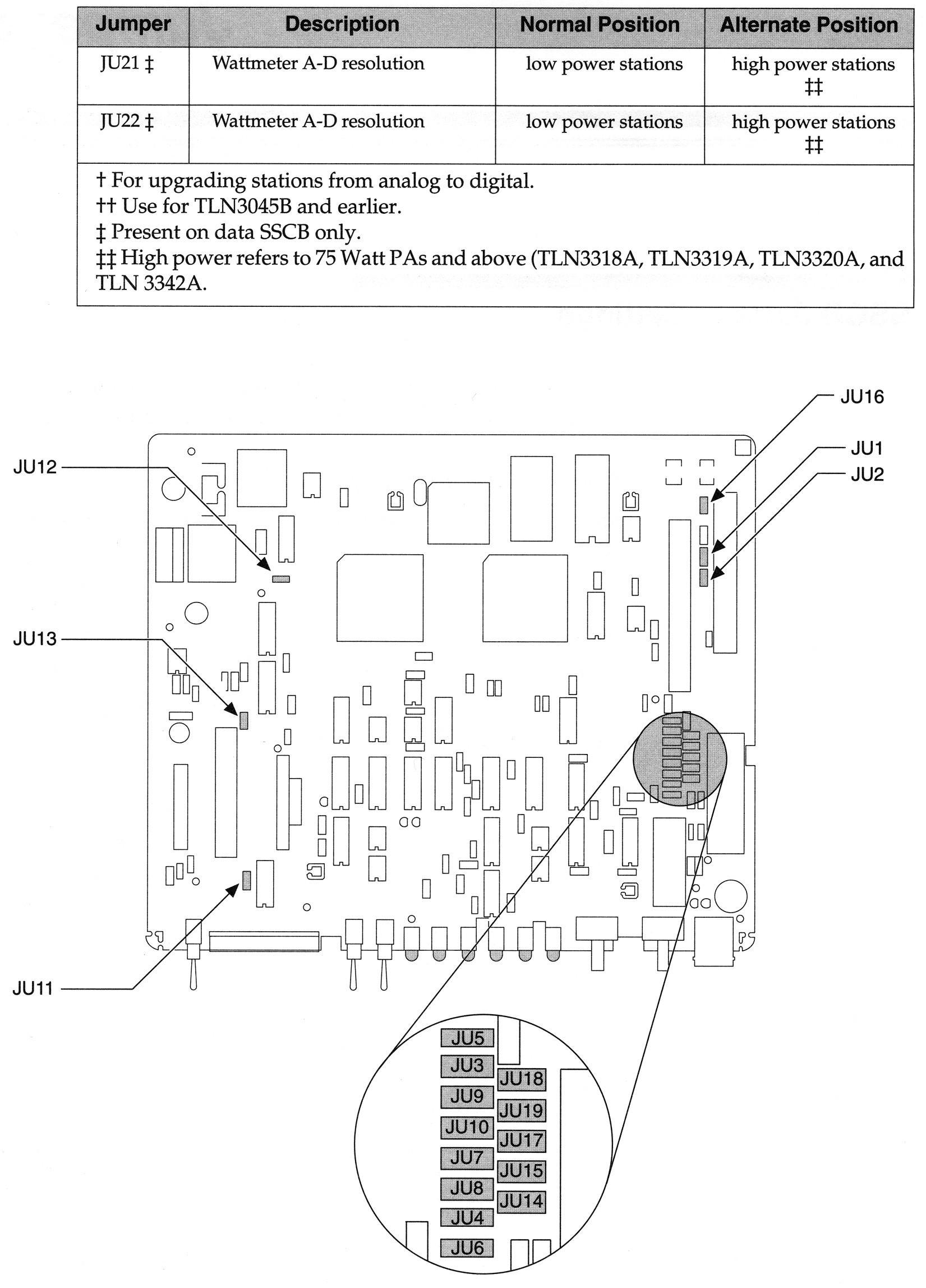
The MSF5000 User Manual has a list of the various SSCB jumpers in Appendix G. These pages are shown below. Note JU13.
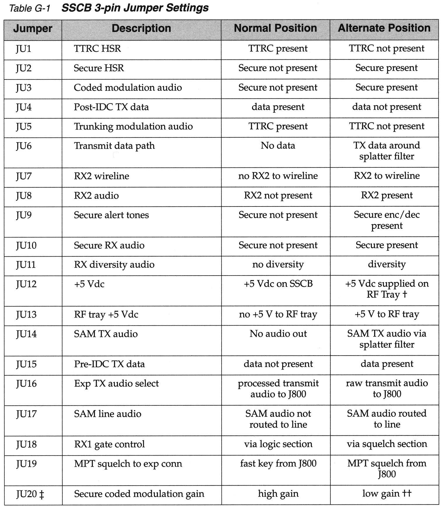
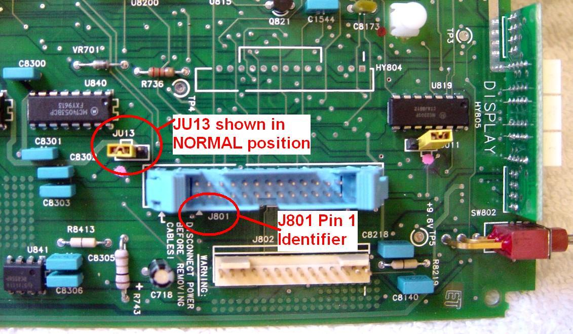
The second page shows the location of the various jumpers on the SSCB. Their location may vary depending on the board revision, so look for JU13 stamped on the board. Also, the documentation doesn't specify which position is "Normal" or "Alternate". Some boards may have arrows pointing to pin 1, while others may have some ink locating the "Normal" position. In the case of JU13, "Normal" is away from the front panel, "Alternate" is towards the front panel and J801. The schematic shows the jumper in its "Normal" position.
Here's a photo of the top of the SSCB with JU13 in its "Normal" position. You can see a small bracket silk-screened above the yellow jumper; this indicates the normal position. The previous owner also painted a pink dot underneath the jumper positions. This is a good thing to do when any board is worked on and the possibility exists that the jumpers could be moved inadvertently.
Acknowledgements and Credits:
The SSCB jumper information came from the current MSF5000 Installation Manual, 6881092E05.
The SSCB schematic came from the current MSF5000 UHF Service Manual, 6881092E80.
Information about the CLB stations was obtained from the MSF5000 UHF CLB Station Manual, 6881062E75.
Some of the conversion information was provided by Bernie KH6IAH.
Marion KC5DPC reported he was able to change the jumper position on one board, and add a wire to another, enabling his SSCBs to work in a CLB station.
Bruce NW5S also reported complete success after moving JU13 on his SSCB.
Contact Information:
The author can be reached at: his-callsign [ at ] comcast [ dot ] net.
Back to the top of the page
Up one level (MSF index)
Up two levels (Motorola index)
Back to Home
This page originally posted on Tuesday 05-Jun-2007.
Article text, artistic layout, photos, and hand-coded HTML © Copyright 2007 by Robert W. Meister WA1MIK.
This web page, this web site, the information presented in and on its pages and in these modifications and conversions is © Copyrighted 1995 and (date of last update) by Kevin Custer W3KKC and multiple originating authors. All Rights Reserved, including that of paper and web publication elsewhere.