Back to Home
By Andy Zorca WJ9J
HTML'd from Andy's information by Mike Morris WA6ILQ

|
Up one level (Scom index) Back to Home |
Expanding the SCOM 7K User Functions By Andy Zorca WJ9J HTML'd from Andy's information by Mike Morris WA6ILQ |
|
The Problem:
I have a fairly complex system, and I was totally out of digital outputs on the S-COM
7K. The Doug Hall RBI-1 Remote Base Interface unit is covered in Chapter 21 of the 7K
manual, and in adition to controlling multiple mobile radios allows one to access
eight more digital outputs (sometimes called user functions, or UFs).
I didn't need remote base control since I wasn't going to connect any remote base radios, but I knew the UF data was in the RBI-1 data stream, somewhere. I developed the circuit below from the schematic of the Advanced Computer Controls FC-1 board (which couples a remote base radio to the ACC controllers). The FC-1 schematic is on the ACC page here at repeater-builder.
I was not trying to redo the FC-1, or trying to support that complex data stream in any way. My only goal was the recovery of the eight UF outputs, and the one chip solution shown below does a fine job of that. One minor problem was that we don't have the use of the ACC FC-1 strobe signal with the 7K, but there is a way around that, presented later.
BTW, the 74C4094 is an 8-bit serial-in/parallel-out shift register, sometimes found as the 74HC4094 or 74HCT4094. A data sheet can be found here.
The Solution:
I built a one-chip circuit that recovers just the eight UF bits from the 48-bit
stream and presents them as TTL levels. NPN switching transistors and some reed
relays did the rest. I created a one-page PDF writeup.
Construction:
Build the circuit on a breadboard and you might want to use an IC socket so when
the lightning hits, well you know......
The 7K is unique in that you do not have to sacrifice any user function outputs
to connect an RBI-1 to the controller.
The circuit will generate all 8 of the User function outputs using the 7K. Since in my application, I did not buffer the outputs, the outputs are high (+5V) when active and Low (0V) when inactive. You could use a Sprague ULN buffer chip like the FC-1 or drive 2N7000 FETs for buffering. The bare 74C4094 is rated to source or sink 25 mA. I would try to keep that under 10 mA.
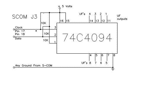
Note that for these to work, you need to enable the RBI-1 mode with:
Enable RBI-1 (PW) 63 71 1 *
Now that the 7K is talking to what it thinks is an RBI-1, we need to
reset the shift register chip with:
Reset RBI-1 (PW) 39 91 *
Now send 1s data to flush any random bits out into the bit bucket:
Set all outputs active: (i.e. +5 on the chip pins)
Send 1s data: (RBPW)12 12345678 *
Now send 0s data to set all bits low:
Set all outputs inactive: (i.e. 0v on the chip pins)
Send 0s data: (RBPW)11 12345678 *
Putting the above command sequence into the power-up macro would be wise.
The last two commands can be customized to set the outputs into whatever
state you want your power-up default to be.
For example, if you wanted to turn on bits 1, 3, and 5 (which are pins 11, 13
and 15 on the 4094 chip) you would use:
(RBPW) 12 1 3 5 *
Note that we are not using the data latch on the chip output, and as such the outputs will ripple or flutter as data flows out of the 7K and through the shift register stages. The 7K is actually sending 48 bits, and the first 40 flow through the shift register and fall into the bit bucket. The shift register is saving the last 8, which happen to be the UF bits. If you need latched data then you can disconnect the strobe pin (pin 1) and add a third 10k resistor from it to +5v, and pulse the chips strobe pin with one of the 7K's own digital output pins in momentary mode (see page 15-2 in the 7K manual). You would then add a "pulse the digital output pin" instruction to the command sequence above. I didn't bother as I was out of digital outputs, plus in my application I was driving relays with NPN driver transistors. I used a 4.7K resistor from the base of the driver transistor to ground, with a 10uf cap in parallel. The cap slows down the switching until the data is stable.
The 7K allows you to group multiple bits into a binary value, i.e. if you needed to output a 6-bit value (zero through 63 decimal) you could "group" 6 of the 8 bits together. This is covered in Chapter 21 of the 7K manual.
Back to the top of the page
Up one level (Scom index)
Back to Home
Copyright © 2007 Andy Zorca WJ9J.
This web page created 24-Dec-2007 by Michael Morris WA6ILQ and the hand-coded HTML
is copyright to WA6ILQ.
This web page, this web site, the information presented in and on its pages and in these modifications and conversions is © Copyrighted 1995 and (date of last update) by Kevin Custer W3KKC and multiple originating authors. All Rights Reserved, including that of paper and web publication elsewhere.