Up two levels (Main Moto Index)
Back to Home
(backplane) Connectors
Compiled by Robert W. Meister WA1MIK

|
Up one level (MTR2000 Index) Up two levels (Main Moto Index) Back to Home |
MTR2000 Rear-of-station (backplane) Connectors Compiled by Robert W. Meister WA1MIK |
|
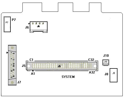
Here's a graphical identification of the various connectors.
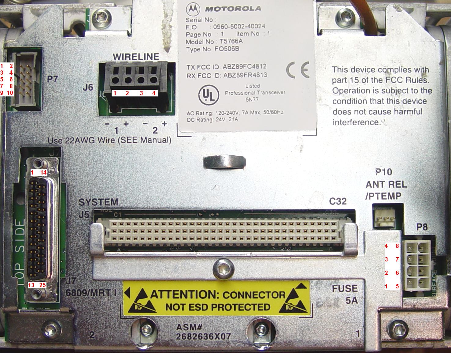
Here's an actual photograph with pin numbers added. Click on any photo for a larger view.
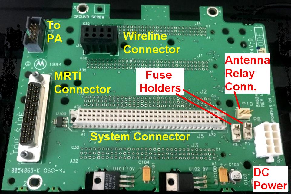
Behind the metal plate is the actual backplane. Here's an annotated photo showing the important items.
The following connectors are located on the front (card-cage side) of the backplane and their designation runs from top to bottom. They are referenced by the tables below but are not detailed further.
The following connectors are located on the back of the station. An asterisk (*) at the end of any signal name in these tables denotes active-low. Notes are indicated as a digit within square brackets [n] and appear at the end of these tables.
Motorola sells a generic System Cable Kit, part number TKN9205A for these stations. This cable provides a housing shell that plugs into the 96-pin backplane connector, 30 loose pins, and a quantity of 24 gauge wires with a pin for the header crimped onto one end.
Notice the screw (in the photo above) holding the cable clamp just below the connector? It's centered exactly on J5 between pin columns 16 and 17. This makes a convenient starting point if you're counting pin numbers when testing the station.
J5 System Connector Row A (lower):
| Pin # | Pin Assignment | I/O | To / From | Signal Characteristics |
|---|---|---|---|---|
| A1 | GPO_8 (WCO) | O | J1-C32, J2-C32 | OCO, 100mA, 40V |
| A2 | PA Fail (Aux I/O) | O | J1-C31, J2-C31 | OCO, 100mA, 40V, active low |
| A3 | SCI_CLCK1 | O | J1-C30, J2-C30, J3-C28 | Do not use. |
| A4 | AC Fail | O | P8-5, J1-C29, J2-C29, J3-C24 | TTL output, active high |
| A5 | GPI_3 (WCI) | I | J1-C28, J2-C28 | Pulled up transistor input, 16V max |
| A6 | GP1_15 (-) (NS) | I | J1-C27, J2-C27 | Negative side opto-isolated input, see C7 |
| A7 | Ext Failsoft (Aux I/O) | I | J1-C26, J2-C26 | Pulled up transistor input, 16V max |
| A8 | GPI_1 (NS) | I | J1-C25, J2-C25 | Pulled up transistor input, 16V max |
| A9 | GPI_2 (NS) | I | J1-C24, J2-C24 | Pulled up transistor input, 16V max |
| A10 | VSWR_Fail* (Aux I/O) | O | J1-C23, J2-C23 | Pulled up transistor output (10kohms to +5Vdc), active low |
| A11 | GPO_2 (WCO) | O | J1-C22, J2-C22 | Pulled up transistor output (10kohms to +5Vdc) |
| A12 | GPO_0 (WCO) | O | J1-B25, J2-B25 | Pulled up transistor output (10kohms to +5Vdc) |
| A13 | Antenna Relay | O | J10-1, J3-C26 | OCO, 200mA, active low |
| A14 | Not Supported | O | J1-C18, J2-C18, J3-C19 | |
| A15 | Spare 310 | - | - | |
| A16 | Spare 308 | - | - | |
| A17 | Aux TX Audio | I | J1-C16, J2-C16, J3-C16 | RSS programmable input sensitivity |
| A18 | Control 14.2 VDC | O | P8 pins 3, 4 (via F2) | +14.2Vdc [1] |
| A19 | GND | - | Station ground | |
| A20 | 5 VDC | O | P8 pins 7, 8 | +5.1 ± 0.25 Vdc |
| A21 | Not Supported | O | J3-C12 | |
| A22 | GP1_7 (WCI) | I | J1-C11, J2-C11 | Pulled up transistor input, 16V max. |
| A23 | Spare 323 | - | - | |
| A24 | Spare 320 | - | - | |
| A25 | Spare 903 | - | - | |
| A26 | Ext PTT or GP1_14 (-), [2] | I | J1-C7, J2-C7 | Negative side opto-isolated input, see A29 |
| A27 | GND | - | Station ground | |
| A28 | GPI_9 (WCI) or GPO_3 (NS) | I/O | J1-C6, J2-C6 | Caution: See Auxiliary I/O section for jumpering information |
| A29 | Ext PTT or GPI_14 (+), [2] | I | J1-C5, J2-C5 | Positive side opto-isolated input, see A26 |
| A30 | AC Fail or GPO_14, [3] | O | J1-C4, J2-C4 | One side of normally open relay, see B29 |
| A31 | GND | - | Station ground | |
| A32 | Control 14.2 VDC | O | P8 pins 3, 4 (via F2) | +14.2Vdc, [1] |
J5 System Connector Row B (middle):
| Pin # | Pin Assignment | I/O | To / From | Signal Characteristics |
|---|---|---|---|---|
| B1 | RX Lock (Aux I/O) | O | J1-B32, J2-B32 | OCO, 100mA, 40V, active high |
| B2 | GPO_13 (WCO) | O | J1-B31, J2-B31 | OCO, 100mA, 40V |
| B3 | RdStat or GPO_15, [4] | O | J1-B30, J2-B30 | One side of normally open relay, see C3 |
| B4 | Carrier Detect Switch | O | J1-B29, J2-B29, J3-B24 | TTL output, active high |
| B5 | GPI_8 (NS) | I | J1-B28, J2-B28 | Pulled up transistor input, 16V max |
| B6 | GPI_5 (NS) | I | J1-B27, J2-B27 | Pulled up transistor input, 16V max |
| B7 | Ext Repeat* (Aux I/O) | I | J1-B26, J2-B26 | Pulled up transistor input, 16V max |
| B8 | Trunk Duplex Enable* | I | J3-B25 | TTL input |
| B9 | GPI_13 (WCI) or GPO_7 (NS) | I/O | J1-B24, J2-B24 | Caution: See Auxiliary I/O section for jumpering information |
| B10 | Spare 311 | - | N/C | |
| B11 | GPI_12 (WCI) or GPO_6 (NS) | I/O | J1-B22, J2-B22 | Caution: See Auxiliary I/O section for jumpering information |
| B12 | GPI_11 (WCI) or GPO_5 (NS) | I/O | J1-B23, J2-B23 | |
| B13 | Spare 301 | - | N/C | |
| B14 | Not Supported | I | J1-B19, J2-B19, J3-B19 | TTL input |
| B15 | GND | - | Station ground | |
| B16 | Spare 300 | - | - | |
| B17 | Spare 321 | - | - | |
| B18 | Control 14.2 VDC | O | P8 pins 3, 4 (via F2) | +14.2Vdc [1] |
| B19 | GND | - | Station ground | |
| B20 | 5 VDC | O | P8 pins 7, 8 | +5.1 ± 0.25 Vdc |
| B21 | RdStat or GPO_15, [4] | O | J1-B12 | OCO, 100mA, 40V |
| B22 | Spare 322 | - | - | |
| B23 | Spare 325 | - | - | |
| B24 | Spare 309 | - | - | |
| B25 | Spare 902 | - | - | |
| B26 | Ext PTT or GPI_14, [2] | I | J1-B7, J2-B7 | Pulled up transistor input, 16V max, see A29 |
| B27 | GND | - | Station ground | |
| B28 | Line 4+ | O | J4-C10 | Wire line output balanced, (+) |
| B29 | AC Fail or GPO_14, [3] | O | J1-B4, J2-B4 | Other side of normally open relay, see A30 |
| B30 | Line 4- | O | J4-A9 | Wire line output balanced, (-) |
| B31 | GND | - | Station ground | |
| B32 | Control 14.2 VDC | O | P8 pins 3, 4 (via F2) | +14.2Vdc, [1] |
J5 System Connector Row C (upper):
| Pin # | Pin Assignment | I/O | To / From | Signal Characteristics |
|---|---|---|---|---|
| C1 | TX Lock (Aux I/O) | O | J1-A32, J2-A32 | OCO, 100mA, 40V, active high |
| C2 | Rdstat-R2 Control | O | J1-A31, J2-A31, J3-A26 | TTL output, high when unsquelched |
| C3 | RdStat or GPO_15, [4] | O | J1-A30, J2-A30 | Other side of normally open relay, see B3 |
| C4 | Failsoft Output (Aux I/O) | O | J1-A29, J2-A29 | OCO, 100mA, 40V, active low |
| C5 | GPI_4 (WCI) | I | J1-A28, J2-A28 | Pulled up transistor input, 16V max |
| C6 | Rx Inhibit | I | J1-A27, J2-A27, J3-B26 | TTL input, active low |
| C7 | GPI_15 (+) (NS) | I | J1-A26, J2-A26 | Positive side opto-isolated input, see A6 |
| C8 | Trunk TX Inhibit* | I | J3-A25 | TTL input |
| C9 | RF Relay Ctrl Out (Aux I/O) | O | J1-B5, J2-B5 | OCO, 200mA, 40V, active high |
| C10 | Ext PTT* Out (Aux I/O), [5] | I | J1-A23, J2-A23, J3-A23 | TTL input |
| C11 | RSSI | O | J1-A22, J2-A22, J3-A22 | Typically 0.5Vdc for -120dBm to 3.5 Vdc for -40 dBm carrier. [6] |
| C12 | GPI_10 (WCI) or GPO_4 (NS) | I/O | J1-A24, J2-A24 | Caution: See Auxiliary I/O section for jumpering information |
| C13 | Spare 304 | - | - | |
| C14 | Not Supported | O | J1-A19, J2-A19, J3-A19 | |
| C15 | GND | - | Station ground | |
| C16 | GND | - | Station ground | |
| C17 | Disc RX Audio | O | J1-A16, J2-A16, J3-A16 | Discriminator audio, flat response. 80mV to 400mV for 60% deviation |
| C18 | Control 14.2 VDC | O | P8 pins 3, 4 (via F2) | +14.2Vdc [1] |
| C19 | GND | - | Station ground | |
| C20 | 5 VDC | O | P8 pins 7, 8 | +5.1 ± 0.25 Vdc |
| C21 | Not Supported | O | J3-A12 | |
| C22 | Spare 302 | - | - | |
| C23 | Spare 324 | - | - | |
| C24 | GPIO_0 (CNTR I/O) | I/O | J1-A9, J2-A9, J3-A17 | TTL input/output |
| C25 | Spare 317 | - | - | |
| C26 | Spare 901 | - | - | |
| C27 | GND | - | Station ground | |
| C28 | Line 3+ | I | J4-C12 | Wire line input balanced, (+) |
| C29 | GPIO_1 (CNTR I/O) | I/O | J1-A4, J2-A4, J3-A13 | TTL input/output |
| C30 | Line 3- | I | J4-A11 | Wire line input balanced, (-) |
| C31 | GND | - | Station ground | |
| C32 | Control 14.2 VDC | O | P8 pins 3, 4 (via F2) | +14.2Vdc, [1] |
NOTES for the above tables:
Commonly Used Signals on J5:
The Ext. PTT Input inhibits the internal Tx PL/DPL signal. All audio, including PL/DPL, must come from another (external) source.
| Name | Description | Pin # | Signal Characteristics |
|---|---|---|---|
| RdStat | TTL compatible logic output indicating Rx. Activation status. | B3, B21, C2, C3 | 0.0 to 0.2Vdc with squelched receiver, 4.8 to 5.2Vdc with un-squelched receiver. |
| Disc. Rx. Audio | Unfiltered and un-squelched discriminator audio without de-emphasis. | C17 | 80mV minimum to 400mV maximum for 60% system deviation. Output level is RSS programmable. |
| RSSI | DC output volts related to received carrier level. | C11 | Typically 0.5Vdc for -120dBm to 3.5 Vdc for -40 dBm carrier. Variation with carrier level @ approximately 40mV/dBm. |
| Cntrl 14.2V | 14.2 volts dc output. For dc-only 250W power supplies, this voltage is equal to the input supply voltage. | A18, B18, C18, A32, B32, C32 | Total current through all of these pins should not exceed 1 amp. |
| 5 V | 5.1 ± 0.25 volts dc output. | A20, B20, C20 | Total current through all of these pins should not exceed 500 mA. |
| GND | Ground. | A19, B19, C19, A27, B27, C27, A31, B31, C31 | Total current through all of these pins should not exceed 1.5 amp. |
| Aux.Tx Audio | Tx. modulation input from external source. | A17 | RSS programmable sensitivity. For R03.01 (host software) and earlier, the fixed sensitivity is @ 172 mVrms for 60% system deviation. RSS programmable for pre-emphasized or flat response. DC offset +2.4V. High impedance input. |
| Ext. PTT | External Tx. keying signal. | C10 | Grounding Ext. PTT pin causes Tx to key. 5.0Vdc on pin when Tx is not keyed. Note: To transmit signaling code (PL / DPL) by external PTT, it should be mapped (via RSS) to Wire line, and external modulation input should be routed to wire line. |
| AC_Fail | Logic output to indicate failure of AC line input. | A4 | Requires a Battery Revert dc supply. Line goes high (5.0Vdc) if AC fails. |
| Wire line Pair 3+/- | Additional wire line for other functions. | C28, C30 | Line sensitivity and operation identical to line pairs 1 and 2. |
| Wire line Pair 4+/- | Additional wire line for other functions. | B28, B30 | Line sensitivity and operation identical to line pairs 1 and 2 |
J6 Wire Line Terminals 1-4:
In the photo of the backplane, the wire line connector on my station is shown pushed up at an angle. It shouldn't be that way; it should come straight out at right angles to the backplane. I have fixed this.
The connector accepts solid wire or stranded wire that's been twisted and tinned. There is NO mating connector. The wires get inserted into the round holes. To release the wires, insert a round tool, a small nail, or another wire into the rectangular hole above the wire. Motorola also sells a Wireline Connector Tool just for this purpose: p/n 6600809D00.
You will need a wire line card installed in your station in order to use the wire line signals. Some stations have them, some don't. This card is usually installed in the uppermost slot of the card cage behind the front panel.
| Pin # | Signal | Usage and Other Notes |
|---|---|---|
| 1 | Line 1- | Tx wire line input for 4-wire configuration. Input level is programmable by RSS between 0 dBm and -50 dBm. Do NOT use this line pair for 2-wire wire line configuration. |
| 2 | Line 1+ | |
| 3 | Line 2- | Rx wire line output for 4-wire configuration. Output level is programmable between +7 dBm and -20 dBm for 100% deviation. Use this line pair for 2-wire wire line configuration. |
| 4 | Line 2+ |
J7 6809/MRTI Connector Pins 1-25:
More information is needed on the MRTI connector signals. The DCV and Notes were obtained by experimenting with a 100w UHF station configured as a repeater with MRTI Enabled.
The various audio signals have a frequency response of about 300 to 3000 Hz, i.e. they won't pass PL/DPL. If specified in the radio's personality, PL/DPL is transmitted along with MRTI Tx Audio when MRTI PTT is grounded.
Remember to use a DC blocking capacitor (10-100uF, 16V) on any audio signal that has DC voltage on it.
If anyone has additional information regarding the signals on the MRTI connector, please pass it on to the author.
| Pin # | Signal Name | DCV | Notes |
|---|---|---|---|
| 1 | MRTI Tx Audio | 2.4 | Pre-emphasized, 0.4V/kHz at 1 kHz |
| 2 | Trunk MRTI PTT* | 5.1 | Ground for Tx (same as pin 11) |
| 3 | Spare | ||
| 4 | MRTI Monitor* | 5.1 | Ground probably disables Rx coded squelch |
| 5 | Spare | ||
| 6 | Spare | ||
| 7 | MRTI Rx Audio | 2.4 | De-emphasized and limited to 3 kHz |
| 8 | Patch Inhibit* or RSTAT | 5.1 | (same as pin 25) |
| 9 | GND | 0.0 | |
| 10 | Aux Carrier* or TSTAT | 5.1 | Low when Tx is on (same as pin 12) |
| 11 | Trunk MRTI PTT* | 5.1 | Ground for Tx (same as pin 2) |
| 12 | Aux Carrier* or TSTAT | 5.1 | Low when Tx is on (same as pin 10) |
| 13 | Trunk Tx Data+ | 3.9 | |
| 14 | Spare | ||
| 15 | MRTI Rx Carrier* | O.C. | Goes to ground with properly coded carrier |
| 16 | GND | 0.0 | |
| 17 | GND | 0.0 | |
| 18 | GND | 0.0 | |
| 19 | GND | 0.0 | |
| 20 | Spare | ||
| 21 | Trunk Tx Data- | 0.0 | |
| 22 | Trunk Rx Audio | 4.8 | De-emphasized and limited to 1 kHz |
| 23 | Trunk Mute* | 5.1 | |
| 24 | PL Strip* or CCI* | 5.1 | Ground disables coded Tx |
| 25 | Patch Inhibit* or RSTAT | 5.1 | (same as pin 8) |
P7 Power Amplifier Interface Pins 1-10:
Orientation looking into the rear of the station:
1   2
3   4
5   6
7   8
9  10
| Pin # | Pin Assignment |
|---|---|
| 1 | Voltage Forward |
| 2 | PA Enable* |
| 3 | PA Reset |
| 4 | V Control |
| 5 | GND |
| 6 | PA D/A CS* |
| 7 | SPI CLK |
| 8 | MOSI |
| 9 | MISO |
| 10 | PA A/D CS* |
J8 Backplane Power Pins 1-8:
This goes directly to the 8-pin connector on the power supply. Orientation looking
into the rear of the station:
4   8
3   7
2   6
1   5
| Pin # | Pin Assignment | Color |
|---|---|---|
| 1 | GND | BLACK |
| 2 | GND | BLACK |
| 3 | +14.2 VDC | GRAY |
| 4 | +14.2 VDC | GRAY |
| 5 | +5 VDC | OR/WH |
| 6 | +5 VDC | OR/WH |
| 7 | GND | BLACK |
| 8 | AC Fail | BROWN |
J10 Antenna Relay Pins 1-3:
Orientation looking into the rear of the station:
1 2 3The external antenna relay connects to pins 1(-) and 3(+).
| Pin # | Pin Assignment |
|---|---|
| 1 | Antenna Relay* |
| 2 | PTemp+ |
| 3 | +14.2 VDC |
While not part of the backplane, this connector feeds DC power to the RF power amplifier and is visible from the back of the station. It is documented here for completeness.
UHF 100 Watt PA Power Connector Pins 1-6:
This goes directly to the 6-pin connector on the power supply. The 40w PAs operate
from 14.2 VDC only. Orientation looking from the rear of the station:
3   6
2   5
1   4
| Pin # | Pin Assignment | Color |
|---|---|---|
| 1 | +14.2 VDC | BLUE |
| 2 | Ground | BLACK |
| 3 | +28.6 VDC | RED |
| 4 | +14.2 VDC | BLUE |
| 5 | Ground | BLACK |
| 6 | +28.6 VDC | RED |
Credits and Acknowledgements:
This information came from the Motorola MTR2000 Basic Service Manual, the MTR2000 Installation and Operation manual, the MTR2000 RSS Help screens and files, and the MTR3000 Basic Service Manual. Additional information, such as wire colors, came from direct examination of a 100w UHF MTR2000 station.
Contact Information:
The author can be contacted at: his-callsign [ at ] comcast [ dot ] net.
Back to the top of the page
Up one level (MTR2000 Index)
Up two levels (Main Moto Index)
Back to Home
This page originally posted on 08-Jun-2011
Article text, photos, and hand-coded HTML © Copyright 2011 by Robert W. Meister WA1MIK.
This web page, this web site, the information presented in and on its pages and in these modifications and conversions is © Copyrighted 1995 and (date of last update) by Kevin Custer W3KKC and multiple originating authors. All Rights Reserved, including that of paper and web publication elsewhere.