Back to Home
Motorola R200X-series
Step Attenuator
By Steve Goggans K7LZJ

|
Back to Moto Test Equipment Back to Home |
Repairing the Motorola R200X-series Step Attenuator By Steve Goggans K7LZJ |
|
I bought an R2008C in 2017. I soon discovered that some dummy had transmitted into the input while it was switched to Monitor instead of Power Monitor. The book says it SHOULD auto-transfer to Power Monitor and sound an alarm. However sometimes it isn't fast enough - case in point. Also well known for many years. This is why I RARELY use the internal dummy load.
There were blown reed relays, diodes, resistors, a mixer, the input attenuator and probably more I forgot. The only thing I couldn't find were chips to repair the RLC Attenuator.
Click on any photo for a larger view.
Taking the Attenuator Apart:
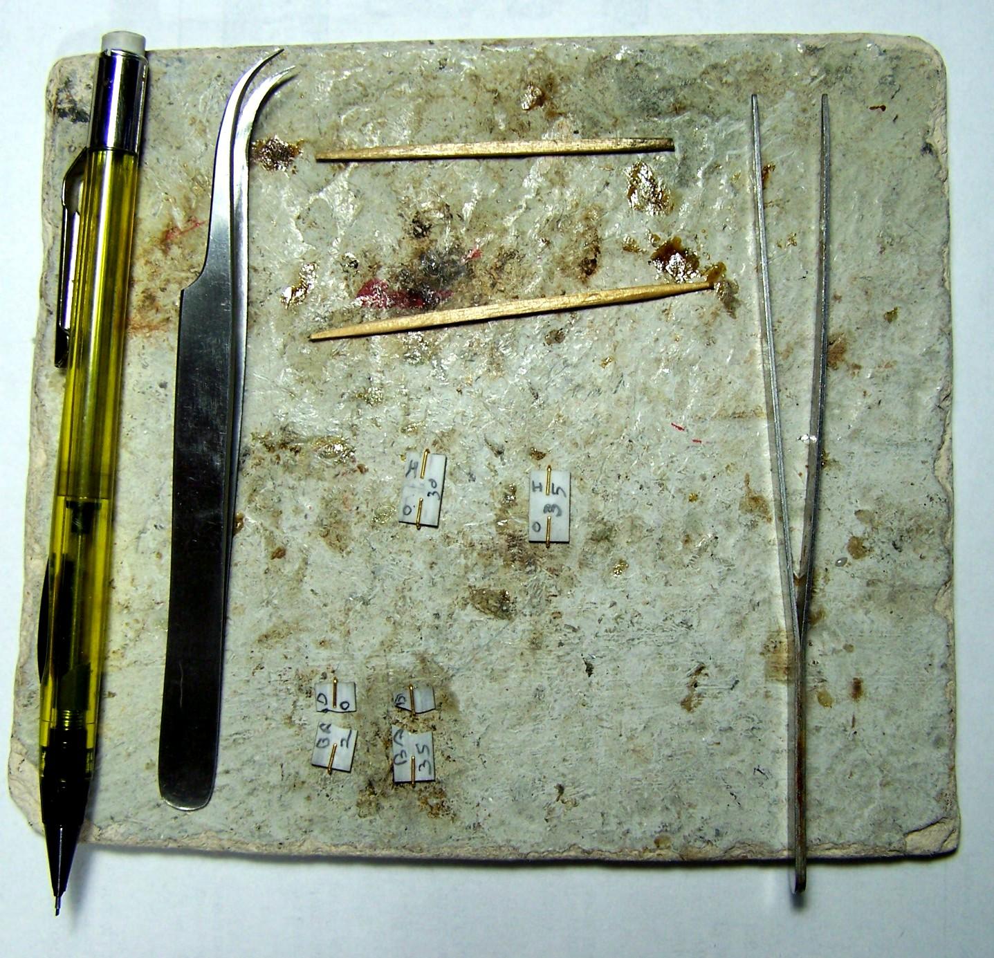
A word of caution in disassembly / top removal: There are tiny springs under the white domes that hold the fingers on the shorting bar. Hold the top on and down while removing the last screws. Carefully place it top down holding it together with plenty of room on all sides. Then slowly pick up the large bottom portion. The thin metal gasket can catch and flip the domes and springs. Put the domes and springs in something like a pill bottle so they can't escape. Make a small diagram showing how all these parts fit together so you can reassemble it later.
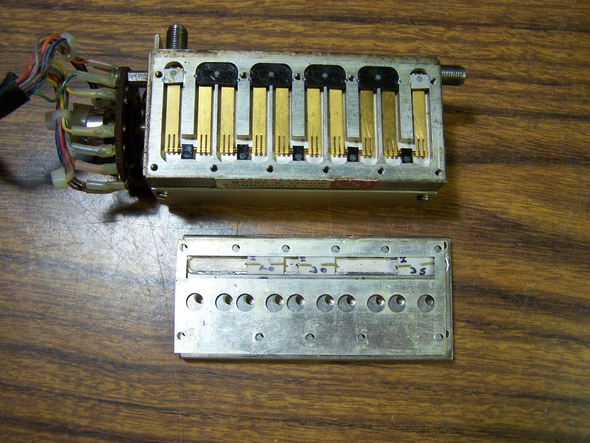
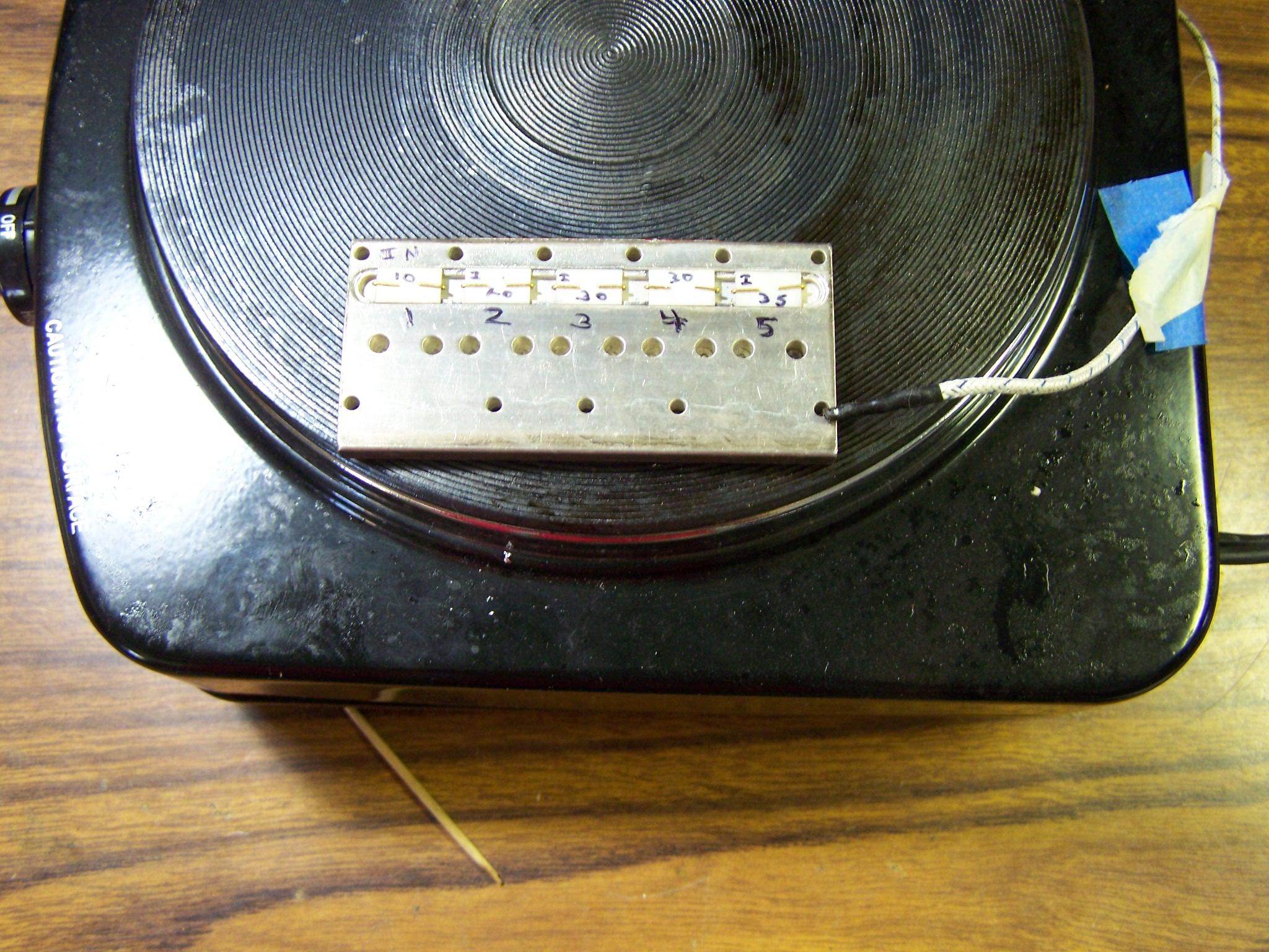
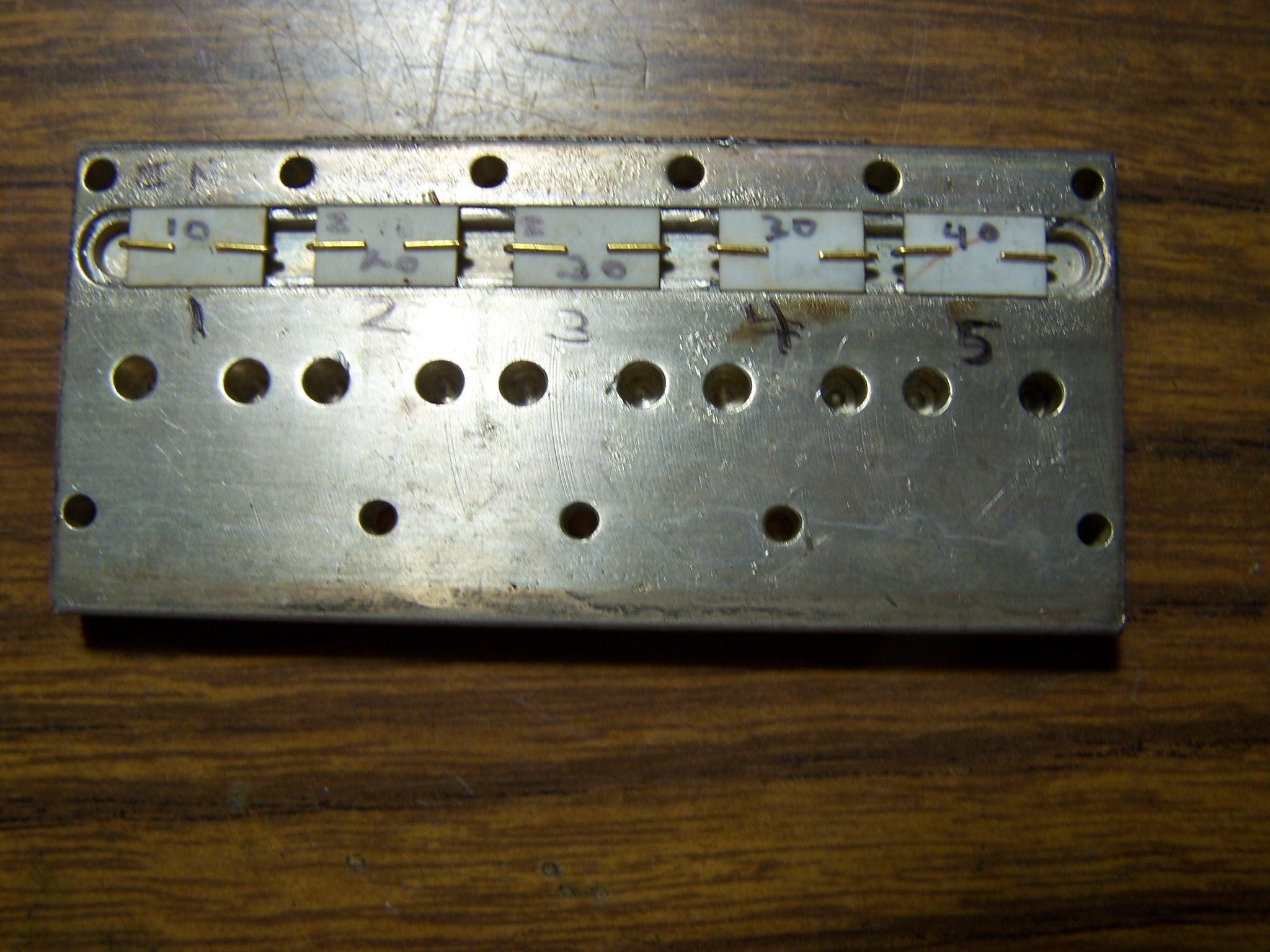
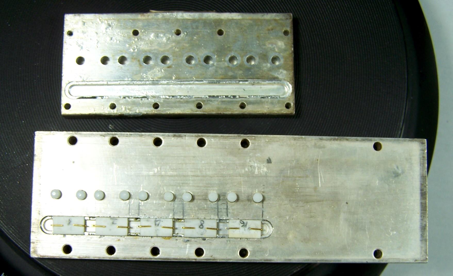
The attenuator is a 5 section unit that has 10, 20, 30, 35, 35 dB chips as ordered from the input end to output end. The 10dB chip (#1) was fried and someone before me broke one of the 35dB chips (#4). (Same dummy?) The photo below shows the attenuator with the 10dB and the first 35db chips removed.
I was able to find other RLC attenuators that had correct chips, other than the 35dB, to cannibalize.
Months on and off were spent looking for currently available chips that would physically fit the assembly. As well as the size problem, there are value problems. I found 30dB and a few 40dB chips but it appears that 35dB chips are a custom value. I found no size / configuration of any value from a current source that would fit. If you know of any current source please email me.
The 130dB step attenuator is Motorola 58-00476N01 / RLC Electronics Model A-2610D.
Extracting the Bad Chips:
Looking at the top of the ceramic chips is not informative. I finally got around to using a hot-air rework station to remove the bad 10dB chip to see what the beast looked like. The ceramic substrate is brittle so I used only a toothpick to try to remove it as I blew hot air on the edges. No luck. "Scotty: We Need More Power!"
The problem of getting enough heat to melt the solder was solved with a hotplate. In fact the rework station wasn't even necessary. 60/40 solder melts at 188C so I got out a temperature meter and stuck the tip of the probe into a screw hole and heated the attenuator silver-plated copper top on a hotplate until it hit 190C and the chip came right out. They are ceramic and brittle. I used a wood toothpick to flip it gently out. Be careful: the gold contact wire solder also melted. See the photo below.
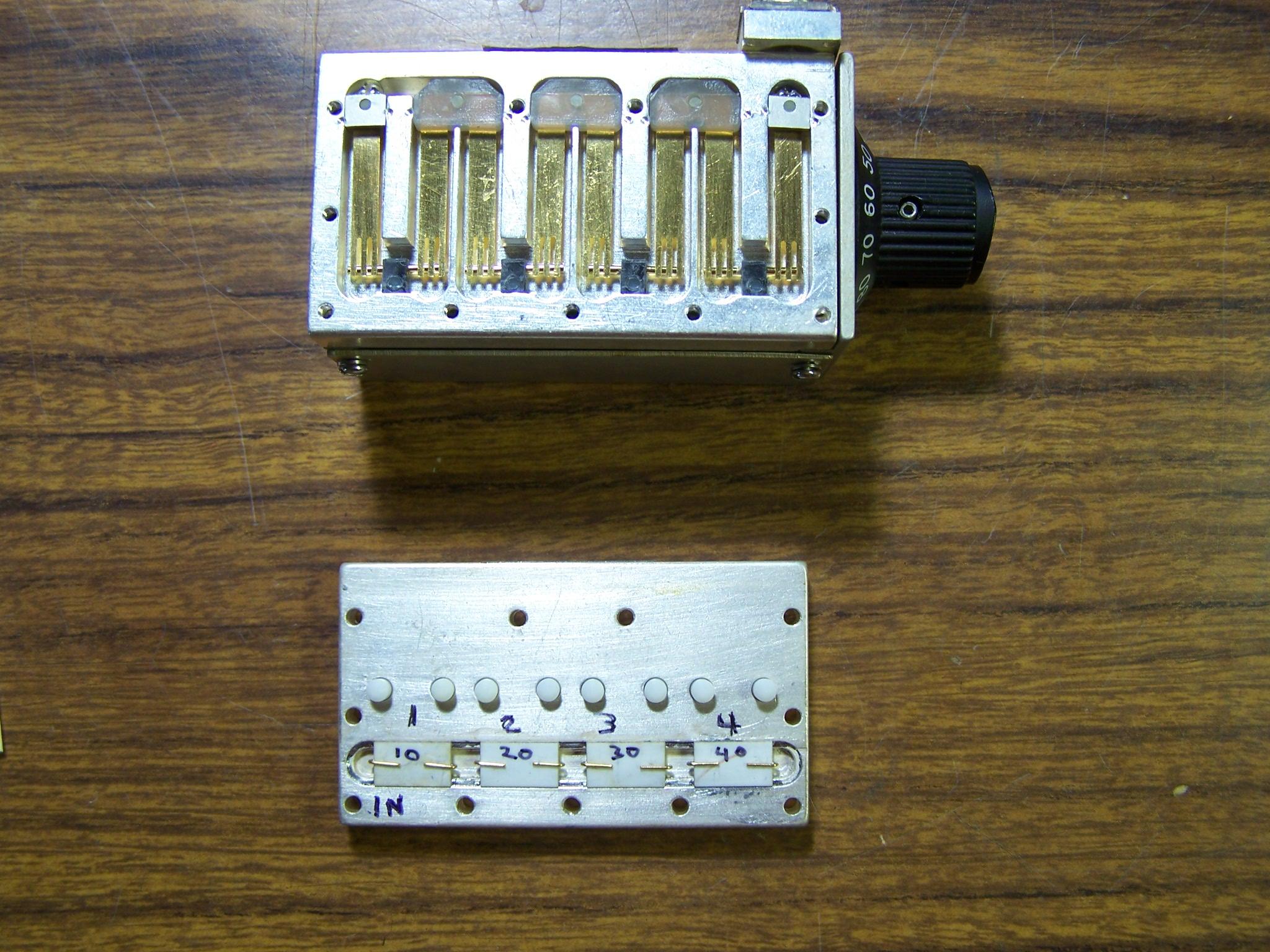
Somehow I hadn't fully comprehended the switching arrangement of the attenuator. Sections 1, 2, and 3 are switched in a binary fashion to produce 0-60dB of attenuation in 10dB steps. Sections 4 and 5 are ALWAYS switched together for another 70dB of attenuation. Standard chips with 30dB and 40dB, instead of the two 35dB chips, would produce the same 70dB and they were in a 4-section unit I got on a popular auction site. See the photo below.
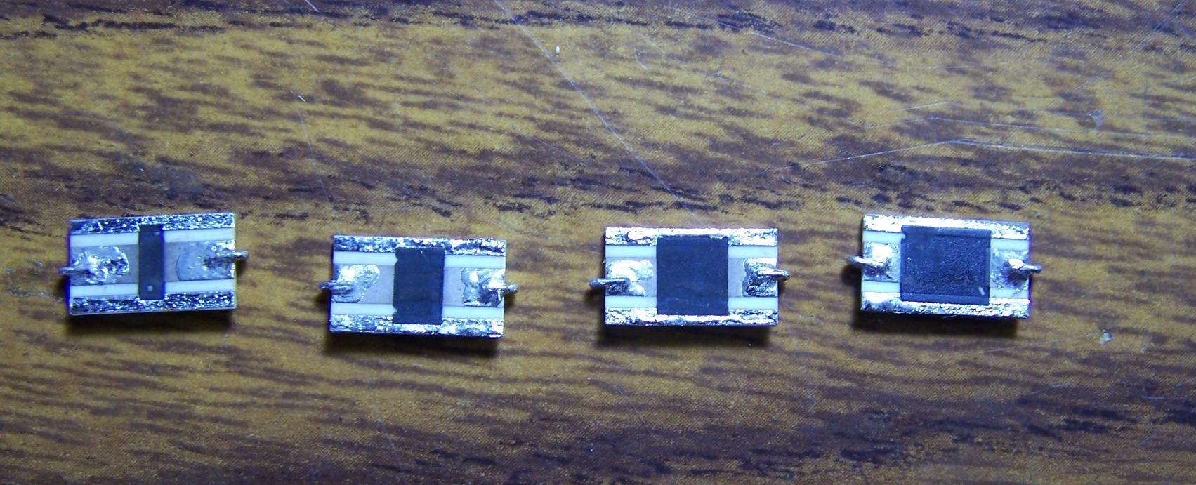
I used a Sharpie marker to mark the chips in dB and how they were oriented towards the input of the donor attenuator. See the photo above. I have no idea why the end towards the input should matter but I kept it the same as originally installed. Somewhere along in this quest I spoke with an engineer at RLC and was told that the chips were individually adjusted by their technicians with (I think he said) a micro blaster.
Here's a photo of the chips I removed from the donor unit pictured above; the 20dB was the only one not used in the repair. They are, from left to right, 10dB, 20dB, 30dB, and 40dB. Notice how the black resistive area in the middle gets larger as the attenuation value increases.
Attenuator Chip Analysis:
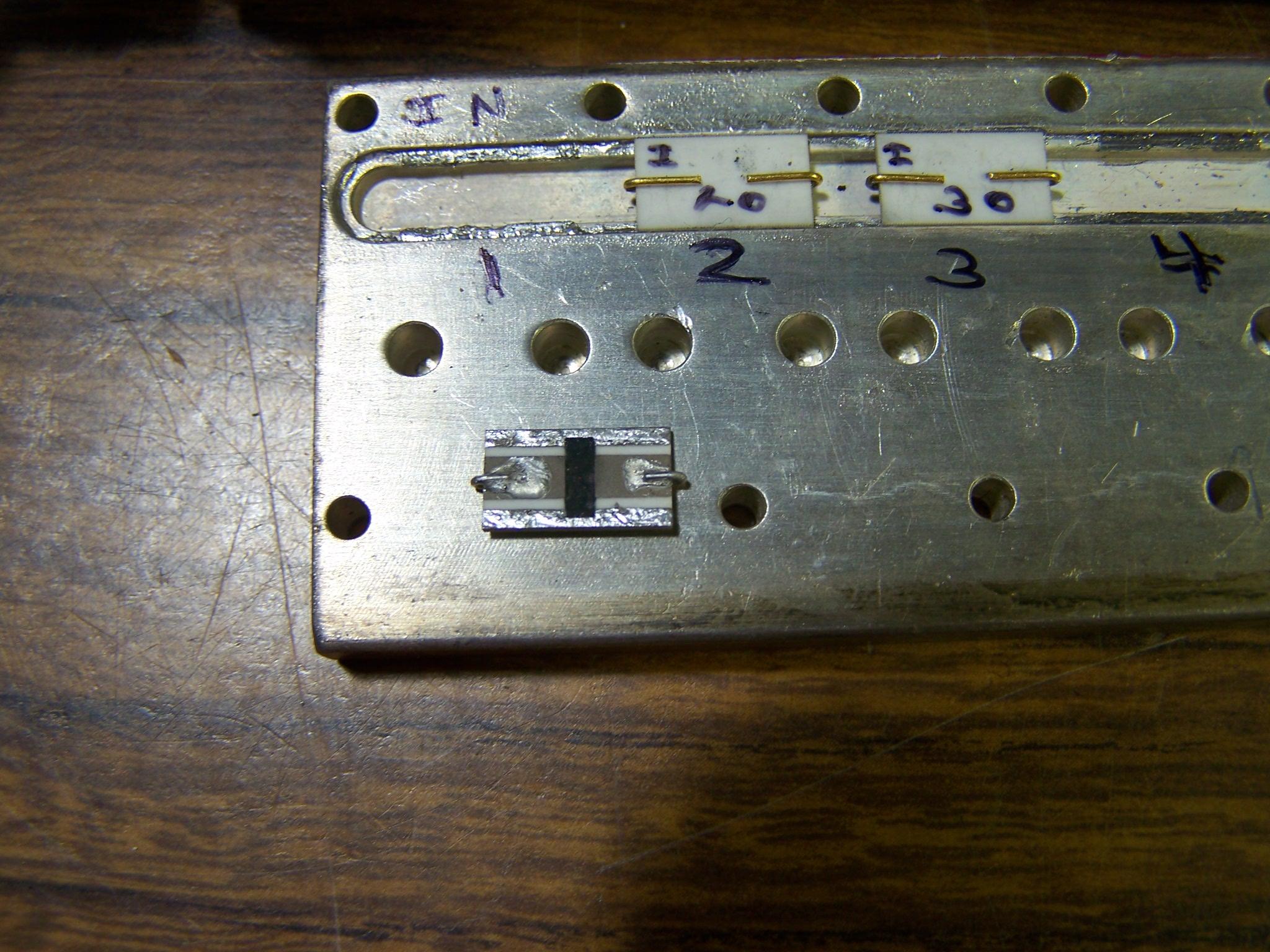
The chips that were removed were measured. See the diagram below for the resistance measurement orientation. These are "pi" pads with the end resistors (to ground) split into two equal value resistors in parallel. Usually the resistance values on the top are equal to the values on the bottom, especially for constant impedance attenuators like these. G1 and G2 are the areas at the top and bottom that were soldered to the mounting plate (ground). I am in a quandary as to the resistance values I found and listed in the table. The measurements were made many times and varied only by 0.1 or 0.2 Ohms. Values are not corrected for lead resistance of around 0.4 Ohms. I used very sharp needle probes and a CAREFUL LIGHT touch probing the gold wires on the chips. The chips were set upside down in the channel in the top for probing.
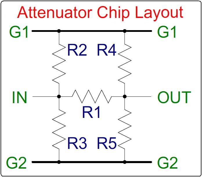
| RLC Attenuator Chip Resistances in Ohms | ||||||
|---|---|---|---|---|---|---|
| Chip dB | R1 | R2 | R3 | R4 | R5 | G1 to G2 |
| 10 | 53.2 | 118.9 | 74.2 | 190.5 | 80.1 | 256.7 |
| 20 | 80.9 | 81.0 | 73.1 | 89.4 | 70.3 | 110.3 |
| 30 | 90.2 | 60.9 | 85.0 | 60.4 | 92.6 | 92.5 |
| 35 | 93.0 | 71.9 | 66.4 | 68.0 | 70.7 | 84.2 |
| 40 | 100.7 | 59.8 | 80.2 | 74.7 | 62.4 | 74.6 |
| BAD 10 | 342 | 373 | 197 | 97.4 | 204 | 268 |
Chip Reinstallation:
Next up was installing the chips. I used an X-Acto knife to GENTLY scrape the bottom edge of the harvested chips to remove any solder that would be wider than the ceramic, so they'd fit into the milled channel from whence they came.
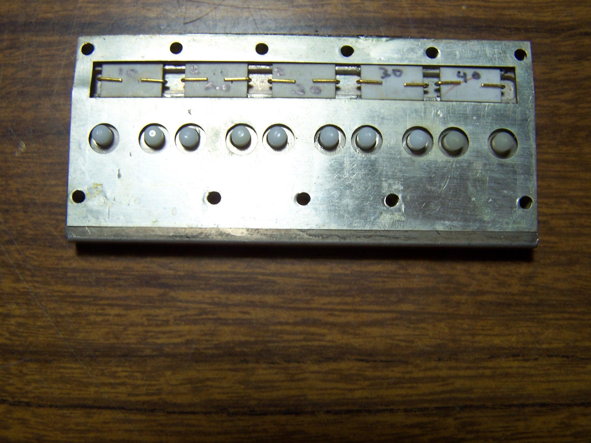
The 10dB and 30dB chips were set in place and the hotplate fired up. Medium is more than enough. At 200C the remaining 35dB chip was removed and the 40dB set in its place. I lined them up by eye, aligning the chip edges to the holes for the springs and insulators. The chips were seated with minimal force using a wood toothpick. See the photo below.
Assembly is reverse of disassembly. WATCH those tiny springs.
See the photo below for the attenuator plate ready to be reattached to the switching mechanism.
Lubing the Step Attenuator: (from my other article)
While at it I decided to look at why the step attenuator was so hard to turn. The 2008C has a mechanical step as the buss interface is Cellular. The 2002 has a switched attenuator because it has the IEEE 488 interface.
The thick cover on the mechanical stepped attenuator with lots of little screws is sort of easy to get to. Avoid the temptation. There are tiny springs and plungers to hold the contacts solidly closed when not activated. Just in case you need a spring, I found one pulled out of a lock cylinder was a dead ringer. The lock was not a Kwikset, but I don't remember the brand. The Attenuator bracket screws can be removed with the input module swung out. The two SMA connectors unscrew and it drops out. The tin cover with 4 screws comes off and there is a camshaft to actuate the switches. It looked like it had never been greased. A bit of thin grease on the cams and plungers made a world of difference.
So, Did It Work?
I measured the resistance looking into the attenuator's input and output connectors with and without a 50 ohm termination, and also the overall measured attenuation in dB. The values are summarized in the table below. The real proof is in the attenuation value, and it's definitely close enough, within ± 1dB. The R2001 manual's specifications for the attenuator are:
| Rebuilt RLC Input Attenuator Resistances | |||||
|---|---|---|---|---|---|
| DB Setting | Input R out open | Input R out term |
Output R in open | Input to Output R | Attenuation in dB |
| 0 | inf | 50.7 | inf | 0.3 | 0 |
| -10 | 79.4 | 48.5 | 119.4 | 51.9 | -9.89 |
| -20 | 54.2 | 47.5 | 64.9 | 77.7 | -19.98 |
| -30 | 50.0 | 48.2 | 53.0 | 89.9 | -30.00 |
| -40 | 48.8 | 48.3 | 49.8 | 94.4 | -39.50 |
| -50 | 47.7 | 47.5 | 48.7 | 94.9 | -50.90 |
| -60 | 48.2 | 48.2 | 48.4 | 96.0 | -61.00 |
| -70 | 48.2 | 48.1 | 49.9 | 97.7 | -70.70 |
| -80 | 48.2 | 48.2 | 49.9 | 97.9 | -80.10 |
| -90 | 47.5 | 47.5 | 49.9 | 97.1 | |
| -100 | 48.2 | 48.2 | 49.9 | 97.8 | |
| -110 | 48.3 | 48.3 | 49.8 | 97.9 | |
| -120 | 47.5 | 47.5 | 49.8 | 97.2 | |
| -130 | 48.2 | 48.2 | 49.9 | 97.8 | |
The -80dB attenuation value was a bit out of probe/sensor range, however you can extrapolate the -70 to -130dB values by adding the -70dB value to the 0-60dB attenuation values. The resistance values are not corrected for around 0.6 Ohm lead resistance and yet the 0dB IN to OUT is 0.3 Ohms tested more than once; I have no explanation. In the "term" column, the output was terminated with an SMA to N adapter and a Bird 50 ohm load. The overall attenuation values beat the specifications.
Additional Hints and Kinks:
I have now done a number of these RLC attenuators and here are a few more helpful ideas and suggestions.
Use a square and pencil to draw fine lines across the face at the edges of all the chips. You need to align them where they were. I find 0.5mm HB lead is great. Write the value on each chip. I also mark "I" for the input end and "O" for the output end of the chips but that most likely is unimportant.
The photo below shows some of the tools I use when working on these units.
Set the hot plate temperature about mid-scale and let it attain temperature. Set the "keeper" close to you and the "donor" behind it oriented in the same direction. See the photo below.
Round toothpicks work great for testing looseness, positioning and lightly seating chips multiple times and again as necessary during cool off. Those ceramic chips will float in the solder.
If the chips aren't loose in a few minutes after setting the tops on the hot plate, turn the temperature up or down. You'll learn the setting.
Once the chips move with a slight touch of the toothpick, lift out the bad one(s) with tweezers. I like fine curved points. The gold contacts are also loose; avoid touching them or reposition as necessary. There is plenty of solder present already; DO NOT add more or the chips will float worse. Move good chip(s) from the donor to the keeper. I remove the extra chips and set them on a hard surface to cool.
CAREFULLY remove the tops to cool. I use larger tweezers. Most chips will float. Lightly go back and forth with a toothpick and LIGHTLY reseat until it cools. When the solder gets almost solid the chips stop floating. Don't keep messing with them or you will make a cold solder joint.
Assemble in a contained area! The little springs under the white domes seem to take flight all by themselves when you install them after the tops are cold.
Test Equipment Used:
Ohmmeter: TWO different Fluke 87 DMMs
Signal Generator: HP-8648
Power Meter: HP-438A
Sensor: 8482A (1.0uW to 100mW) that's -30dB to +20dB into 50 Ohms.
Sensor: 8484A (0.3nW to 10uW) that's -68dB to -20dB.
Maximum output for the signal generator is +14dB.
SMA to double banana adapters were used at each end of the attenuator.
Contact Information:
The author can be contacted at: k7lzj [ at ] arrl [ dot ] net.
Back to the top of the page
Back to Moto Test Equipment
Back to Home
This web page created 07-Nov-2019
Article text, layout, and photos © Copyright 2019 by Steve Goggans K7LJZ.
Additional text, chip diagram, and article conversion © Copyright 2019
by Robert Meister WA1MIK.
This web site, the information presented in and on its pages and in these modifications and conversions is © Copyrighted 1995 and (date of last update) by Kevin Custer W3KKC and multiple originating authors. All Rights Reserved, including that of paper and web publication elsewhere.