Back to Home
Jumper Cards for the
Motorola R2001-series
Communications Systems Analyzers
By Steve Goggans K7LZJ and
Robert W. Meister WA1MIK

|
Back to Moto Test Equipment Back to Home |
IEEE and Cellbus Jumper Cards for the Motorola R2001-series Communications Systems Analyzers By Steve Goggans K7LZJ and Robert W. Meister WA1MIK |
|
Background:
In the R20XX A/B/C models, slot A8 is reserved for an IEEE board, although later C models could also accept a Cellular Telephone Test board. If this board is removed or the model number indicates it didn't have IEEE capability, a short jumper board must be inserted into the motherboard socket to pass about a dozen signals through the missing board. Without this jumper board, the service monitor will not function properly, if at all.
Steve is pretty sure that almost all R2008C units have the Cellbus card. This is a special case and Steve is working on bypassing the Cellbus card A8. So far he's determined the same four signals, that the D jumper cards bypass, are required for the Cellbus card, just on the appropriate pins for the C model. If you have a bad A8 that you need to remove, email Steve.
The R20XX D models have two slots, one for a Cellular Telephone Test board or a SecureNet board or a Trunking Radio Test board (in slot A12 or slot A13) and one for an IEEE board (always in slot A13). If either board is removed or not present, an appropriate jumper board must be inserted to pass signals through the missing board. These boards are vastly different from the board used in the A/B/C models and only deal with passing three or four signals.
We will cover the A/B/C (slot A8) jumper board first, followed by the D (slots A12 and A13) jumper boards.
R20XX A/B/C Jumper Board:
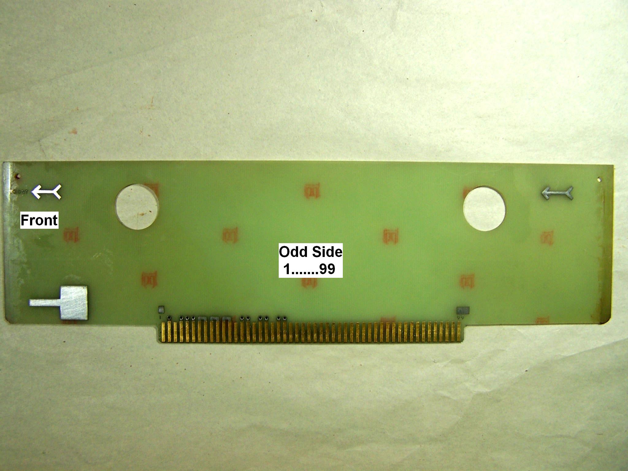
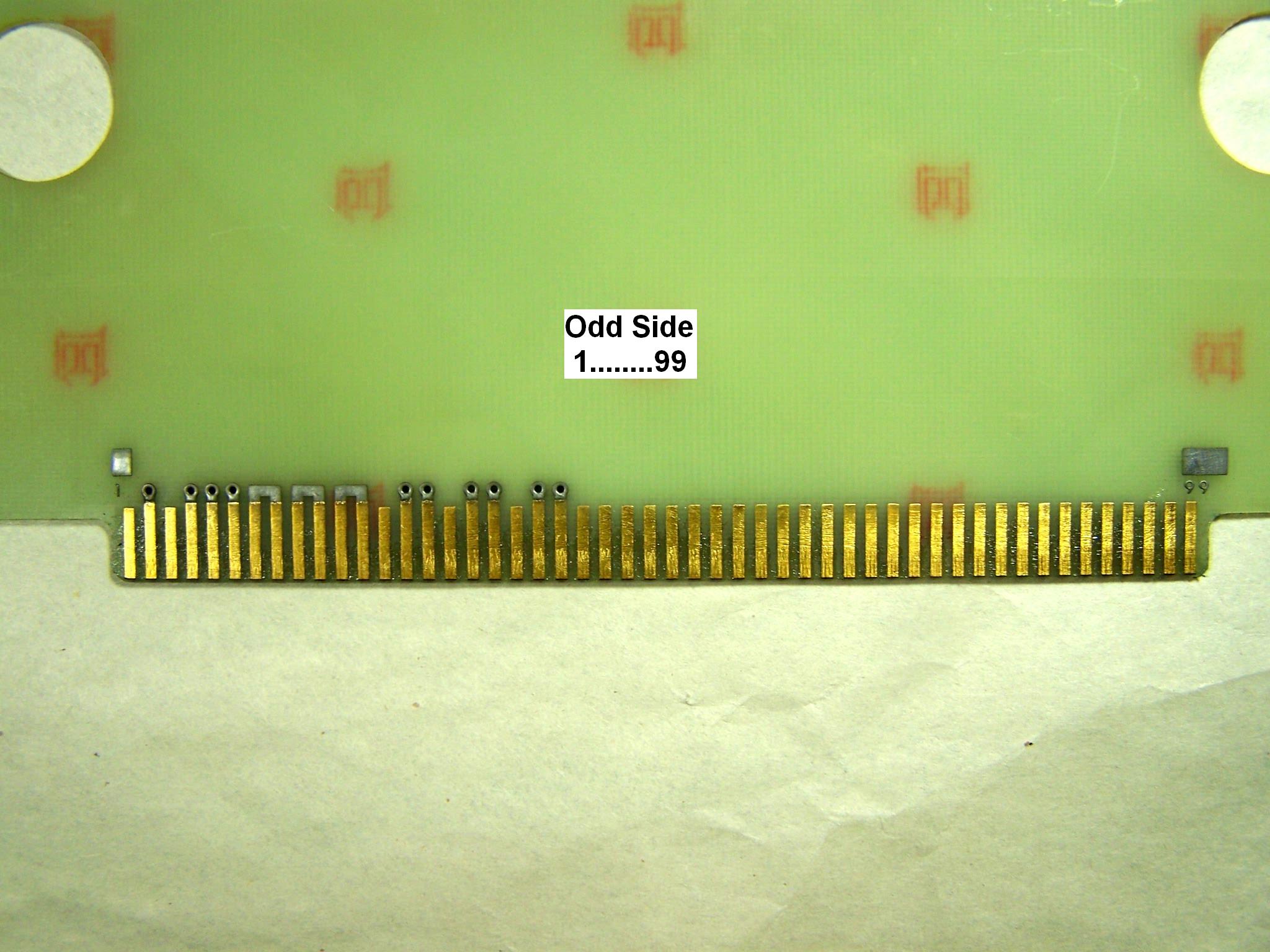
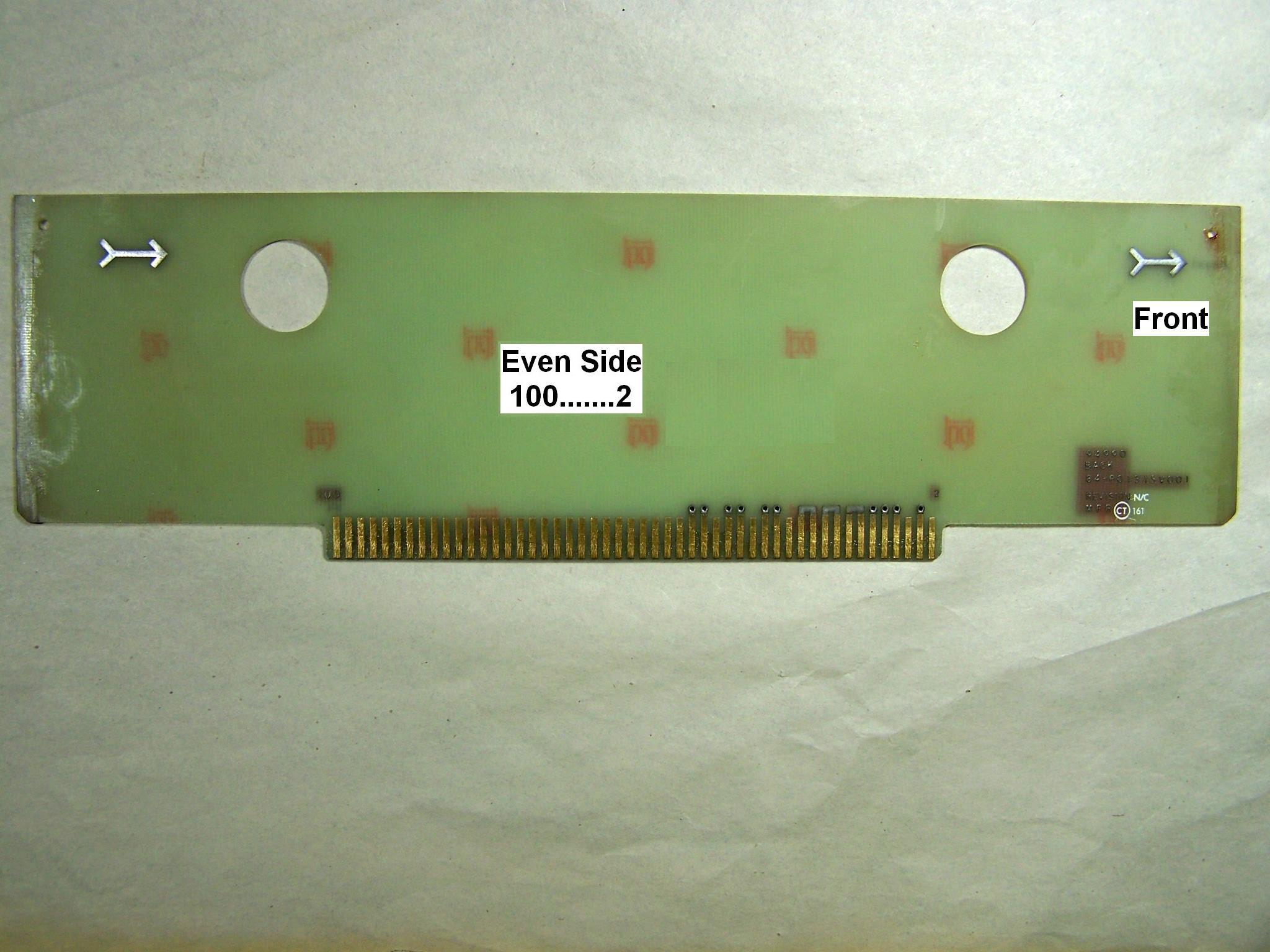
The jumper board is a short full-width board with 100 pins, 50 on each side, labeled 1-99 for the odd side, and 2-100 for the even side. Arrows and the word "FRONT" are etched into the board and point towards the front of the service monitor. Pin 1 is towards the front of the service monitor. Here are full-width and detailed photos for each side of the jumper board. Click on any photo for a larger view.
First up is the full-width odd side.
Next we have the detailed odd side.
Then we have the full-width even side.
Last we have the detailed even side.
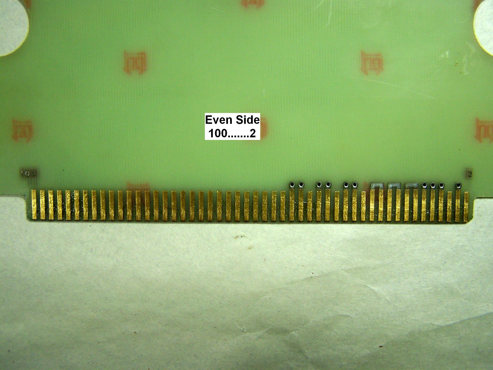
You can see that some adjacent pins on each side are connected together. You can also see feed-through holes that connect a pin on the odd side to a higher numbered pin on the even side. The table below documents the various interconnected pins and signals on the stock jumper board for the various models. The A, B, and C models use the same jumper board.
| Connect | ABC | Signal Name |
|---|---|---|
| 3 to 4 | X | AM MOD + DC REF (I) / (O) |
| 7 to 8 | X | BFO Frequency |
| 9 to 10 | X | BFO on / off |
| 11 to 12 | X | 0 to 10 MHz offset select |
| 13 to 15 | N/C MOBO | |
| 14 to 16 | X | 45 MHz offset select |
| 17 to 19 | N/C MOBO | |
| 18 to 20 | X | Offset Fine Tune |
| 21 to 23 | N/C MOBO | |
| 22 to 24 | X | Offset Coarse tune |
| 27 to 28 | X | 1 kHz SINE (I) / (O) |
| 29 to 30 | X | 1 kHz SINE (I) / (O) |
| 33 to 34 | X | EXT MOD (I) / (O) |
| 35 to 36 | X | EXT MOD RTN (I) / (O) |
| 39 to 40 | X | INT MOD (I) / (O) |
| 41 to 42 | X | INT MOD RTN (I) / (O) |
Abbreviations used in the table above:
(I) = Input.
(O) = Output.
RTN = Return.
N/C = Not Connected.
MOBO = Motherboard.
R20XX D Jumper Boards:
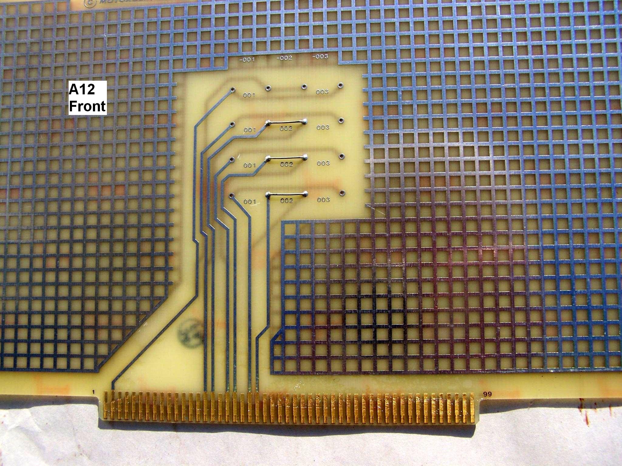
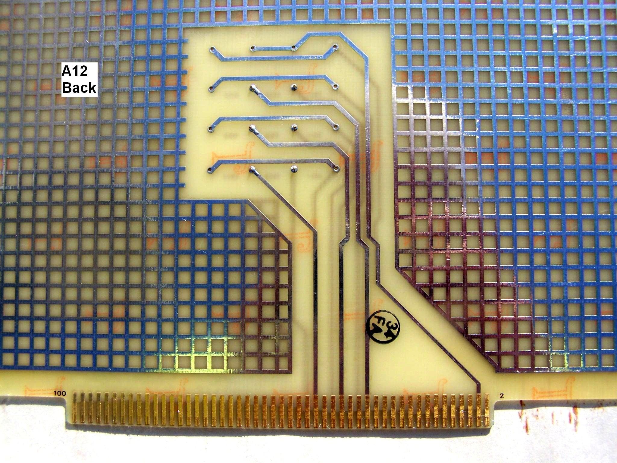
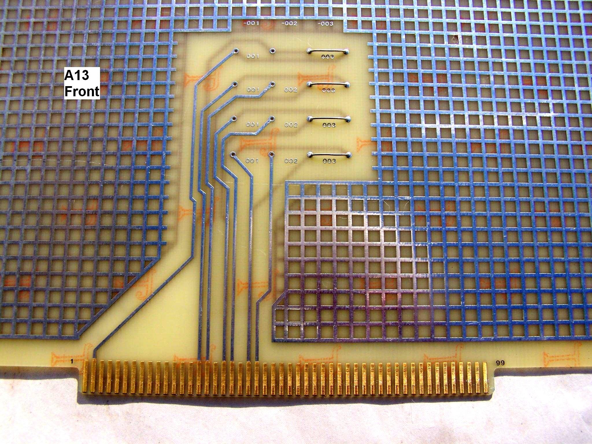
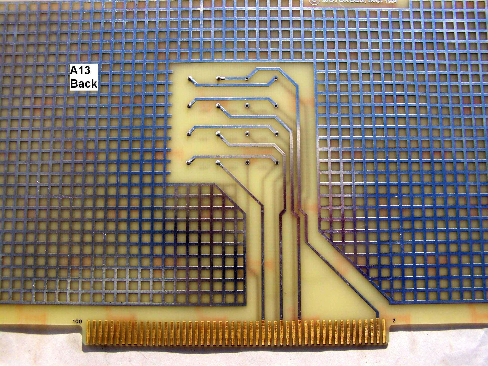
The same double-sided board is used for A12 and A13 jumper boards in the D series. Three or four jumpers are inserted into holes to connect the various signals depending on whether the board is to be placed in slot A12 or slot A13. There are four rows of jumpers with three possible jumper positions in each row. Only one position is jumpered per row. The rows are NOT identified but I've named them "A" through "D" starting at the top. The columns are NOT identified but I've named them "1" through "4" starting at the front, or pin 1/2 end. The three jumpers in each row connect columns 1-2, 2-3, and 3-4. These jumper positions are also identified on the front as "001", "002", and "003".
| Pin | Row | Column | Signal Name |
|---|---|---|---|
| 3 | A | 1+4 | AM MOD + DC REF (I) |
| 29 | B | 1+4 | 1 kHz SINE RTN (I) |
| 31 | B | 2 | 1 kHz SINE RTN |
| 35 | C | 1+4 | EXT MOD RTN (I) |
| 37 | C | 2 | EXT MOD RTN |
| 41 | D | 1+4 | INT MOD RTN (I) |
| 43 | D | 2 | INT MOD RTN |
| 4 | A | 2+3 | AM MOD + DC REF (O) |
| 30 | B | 3 | 1 kHz SINE RTN (O) |
| 36 | C | 3 | EXT MOD RTN (O) |
| 42 | D | 3 | INT MOD RTN (O) |
Abbreviations used in the table above:
(I) = Input.
(O) = Output.
RTN = Return.
For the A12 jumper card, jumper points B2-B3 (1 kHz SINE RTN to 1 kHz SINE RTN (O)), C2-C3 (EXT MOD RTN to EXT MOD RTN (O)), and D2-D3 (INT MOD RTN to INT MOD RTN (O)). Only these three signals need to be fed through if a board is not present. The photos below show the front (odd numbered) and back (even numbered) sides of an A12 jumper card.
For the A13 jumper card, jumper points A3-A4 (AM MOD + DC REF (I) to AM MOD + DC REF (O)), B3-B4 (1 kHz SINE RTN (I) to 1 kHz SINE RTN (O)), C3-C4 (EXT MOD RTN (I) to EXT MOD RTN (O)), and D3-D4 (INT MOD RTN (I) to INT MOD RTN (O)). Only these four signals need to be fed through if a board is not present. The photos below show the front (odd numbered) and back (even numbered) sides of an A13 jumper card.
Acknowledgements and Credits:
Steve Goggans K7LJZ took all photos and developed the table as an XLS file.
Signal names came from several R2001 communications service monitor manuals. Pin connections came from inspection of the actual jumper boards.
Robert W. Meister WA1MIK wrote all text.
Contact Information:
Steve can be contacted at: his-callsign [ at ] arrl [ dot ] net.
Bob can be contacted at: his-callsign [ at ] comcast [ dot ] net.
Back to the top of the page
Back to Moto Test Equipment
Back to Home
This web page created 07-Aug-2020
This web site, the information presented in and on its pages and in these modifications and conversions is © Copyrighted 1995 and (date of last update) by Kevin Custer W3KKC and multiple originating authors. All Rights Reserved, including that of paper and web publication elsewhere.