Back to Home
D-series Power Supply
By Steve Goggans K7LZJ
and Robert W. Meister WA1MIK

|
Back to Moto Test Equipment Back to Home |
Repairing the Motorola R20xx D-series Power Supply By Steve Goggans K7LZJ and Robert W. Meister WA1MIK |
|
Background:
This article came about because no information was available about the thermistors used on the LVPS A3 board in the R20 D-series service monitors.
The unit in question is a R2008D. The serial number date code identifies it as being made during the second half of January 1987, however the EPROMs have dates of 06/1995.
The LVPS high-voltage supply, as well as the battery charger and ovenized oscillator power (all on A3) is energized when the unit is plugged in. The thermistors limit the capacitor charging current to protect the diode bridge and everything ahead of it. Incoming AC (120V or 240V) is converted to 330VDC, which supplies a switching circuit (on A6) feeding a transformer (on A5), which produces multiple AC voltages that are rectified and filtered (also on A5) to provide DC to the rest of the unit. External DC or a battery pack supplies power to a second switching circuit (on A6) feeding the same transformer above to produce the DC voltages. Control and switcher drive is done on A4.
Click on any photo for a larger image.
Why It's On The Bench:
The unit had been plugged in but turned off for a long time (days or weeks) when suddenly... POOF. Both thermistors were totally destroyed and board somewhat charred. The unit arrived with the power filter replaced, RT1 and RT2 removed, and the A3 board had not been cleaned.
The original parts were blue disc thermistors, RT1 and RT2 on the A3 card, with a part number of 0680342B85 with no other description in the manual.
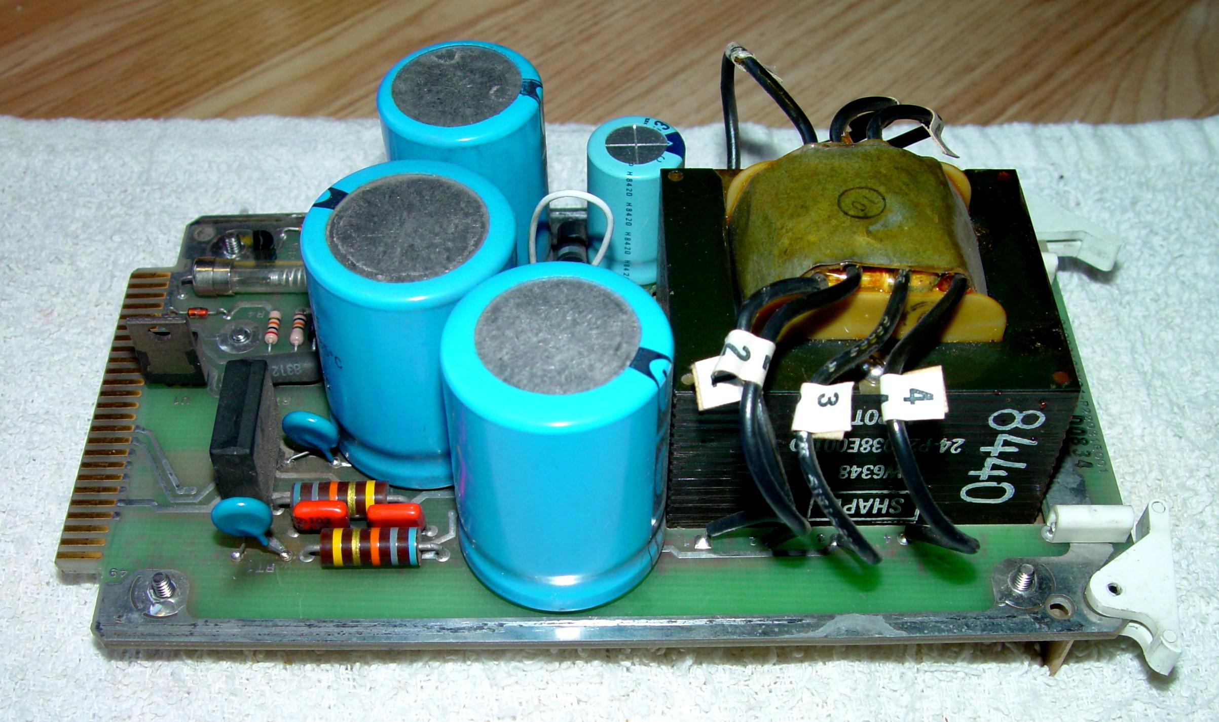
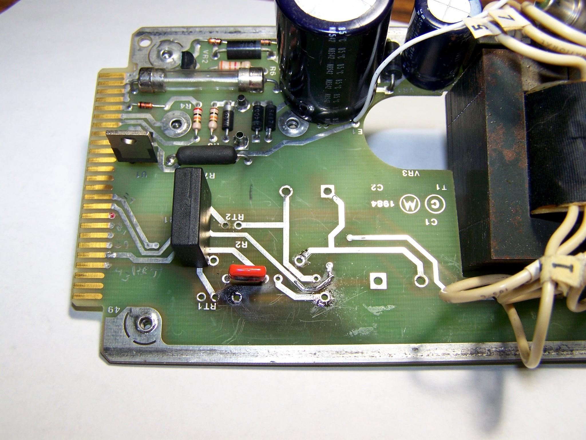
Bob and I spent considerable time trying to identify them. A unit Bob had access to, had two unmarked blue thermistors, so that was no help. They had a lead spacing of 7 mm and measured 9 mm diameter by 2.5 mm thick and had 12 to 13 Ohms of resistance at 78F. Here's a photo showing that area of the circuit board.
And from the other side.
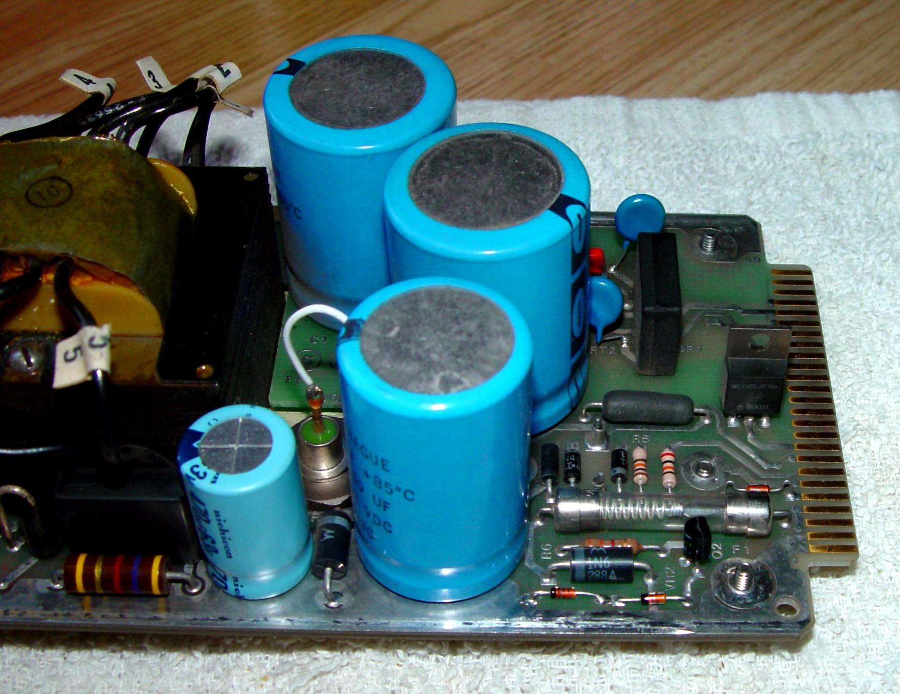
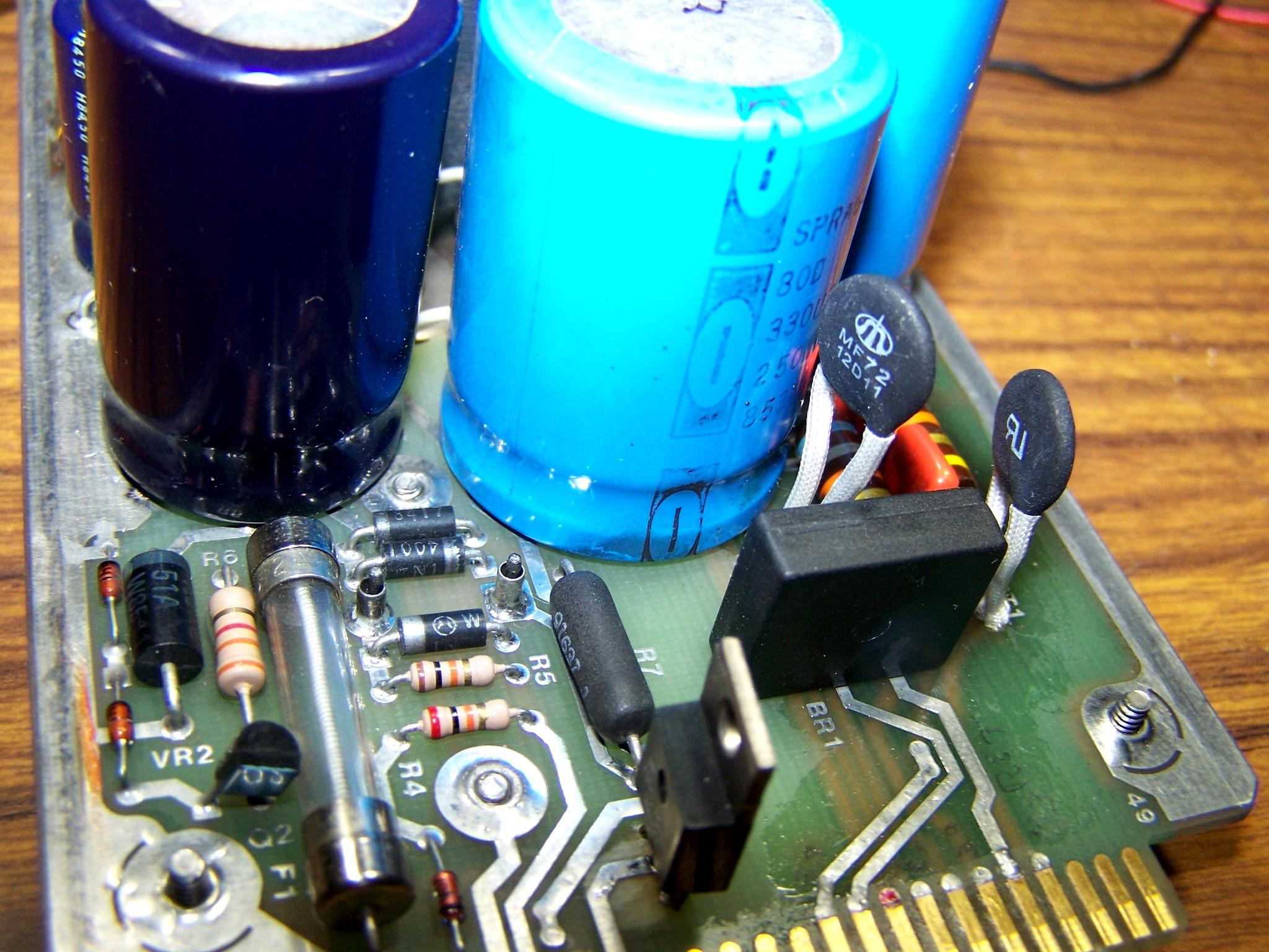
Apparently the parts used on newer D-series A3 boards are physically smaller and have narrower lead spacing. A 21D with EPROMs dated 03/1995 has the same 2.5 mm lead spacing, are 9 mm diameter by 3.3 mm thick, and have 11.3 and 10.8 Ohms of resistance at 78F. Notice these are similar to the ones above but the lead spacing is much closer, implying a revision was made to the component layout on the A3 card. Here's a photo showing that area of the circuit board.
Analyzing The Circuit:
First order of business was to find out the steady-state current supplied by the high voltage section. A pair of 1 Ohm resistors were inserted in place of RT1 and RT2 and the incoming AC voltage was slowly brought up with a Variac. The steady-state current, derived from the voltage across the 1 Ohm resistors, is around 500 mA.
Next order is finding the diode bridge specification. Fortunately it has a part number KBL06 stamped on it. The parts list said the ratings were 600V and 4A; the part number lookup said it had a 200A surge current rating. When set for 120VAC input, two diodes in this bridge are used as a voltage doubler, developing about 330VDC. When set for 240VAC input, the entire bridge is used as a full-wave rectifier, developing the same 330VDC. This type of bridge/doubler arrangement is very common in 120V/240V switching power supplies. Most PC power supplies are designed this way.
Without going overboard, the surge current is limited both by the thermistors and physical mounting and wiring, AC cord plug and socket resistance, AC fuse, input line filter, internal wire size and length, board connector resistance, circuit board trace width and length. The unit has a 3A fuse in the AC line for operation from 120VAC.
Dealing With The Damage:
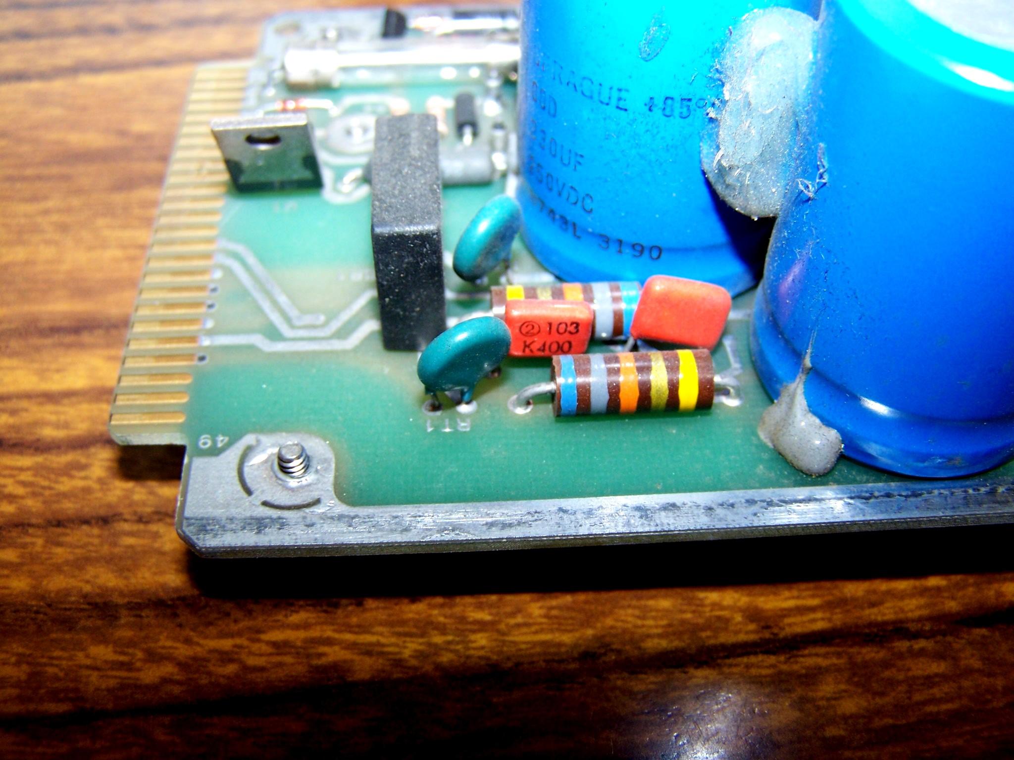
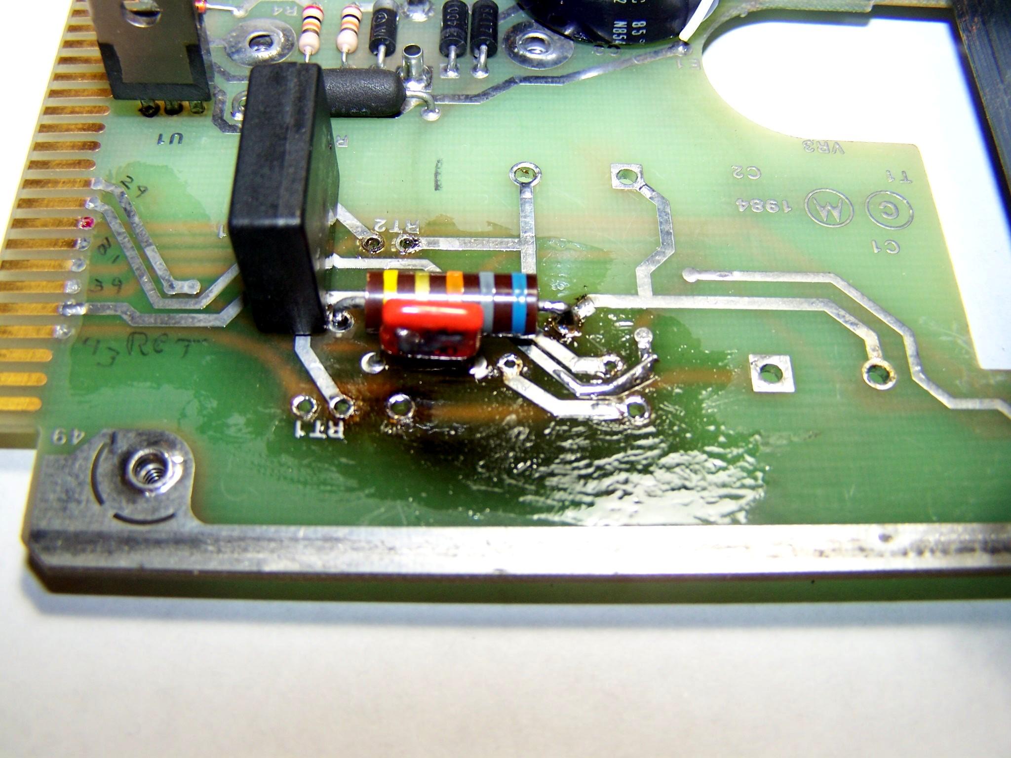
The board did not clean up well with my favorite scrubbing bubble treatment and I wanted to verify some component values. It was fortunate that R1 and R2 were removed for measurement. The trace beneath R1 was almost arc burned in half. It is unlikely the damage would have been noticed otherwise. Here's a photo of the board with several parts removed. The circled areas were where the arc occurred; the bigger trace had burned through.
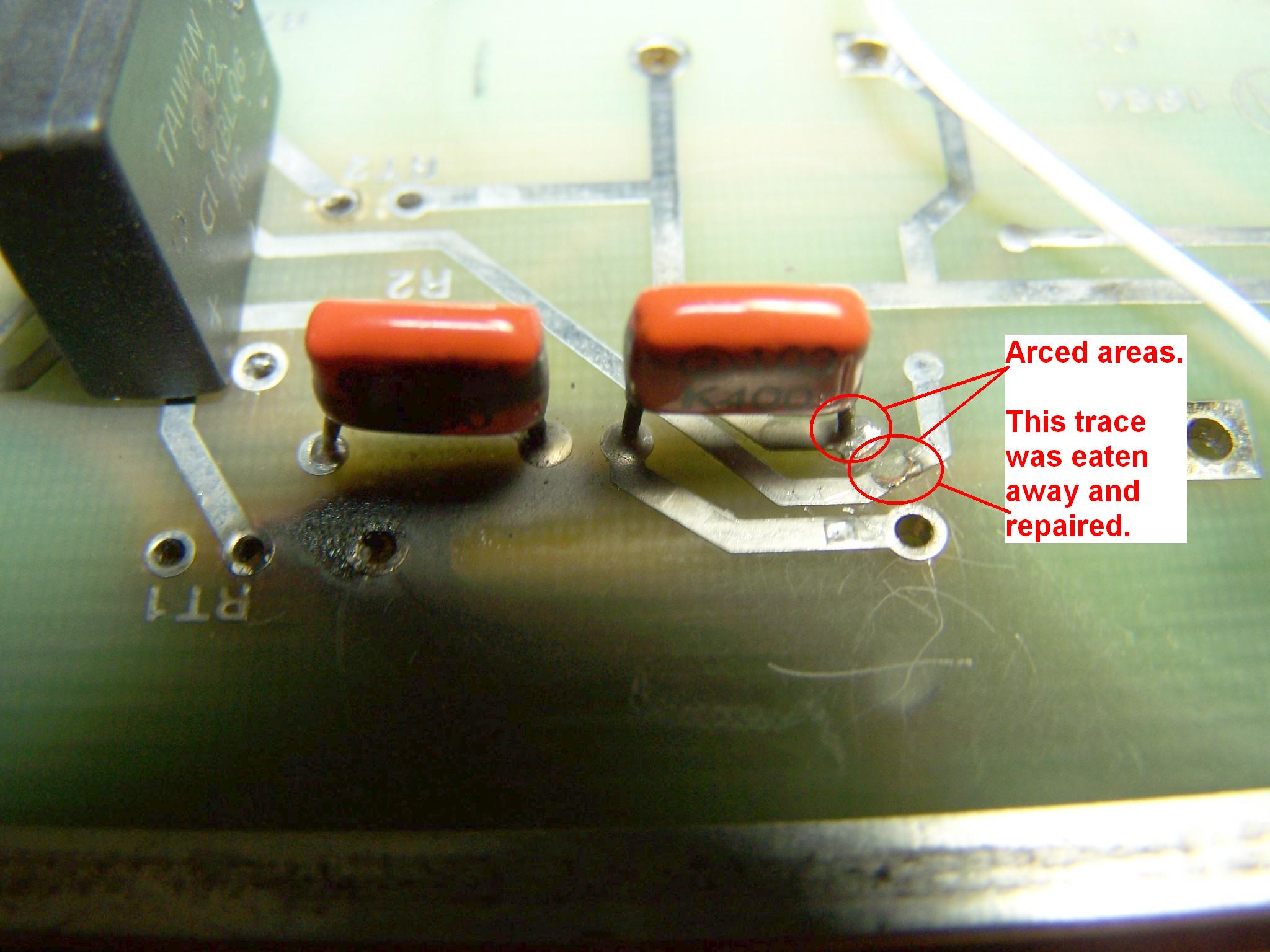
The arc burn in the photo of bottom of A3 is between pin 31/32: Primary 2 and pin 41/42: 110 Return. Trace spacing seemed mighty close and I wondered if this was a problem. I called a knowledgeable friend who had retired from the Motorola Service department. His response was he never recalled the service department receiving a totally dead D series. So I gave up worrying about the trace spacing.
The trace in the damaged area of the photo above was repaired with a short piece of #30 wire wrap wire. The board was defluxed and any carbon or residue from the blown thermistors was scraped off. The repair is visible in the photo below.
The front and back of the circuit board around the area of failure was coated with clear air-dry insulating varnish. Here's a photo of the coated board.
Selecting Suitable Thermistors:
I tried several different thermistors and recorded the 1 ms peak voltage readings across them with a Fluke 87 DMM. Using their cold resistance to derive 1 ms peak current, the cold resistance taken from both styles used implied the use of 10 to 12 Ohms cold resistance, which seems quite conservative and was in the range of resistance measured on factory boards. I ended up using MF72-012D11 12 Ohm 3A thermistors. Here's a photo showing those thermistors installed in the repaired board.
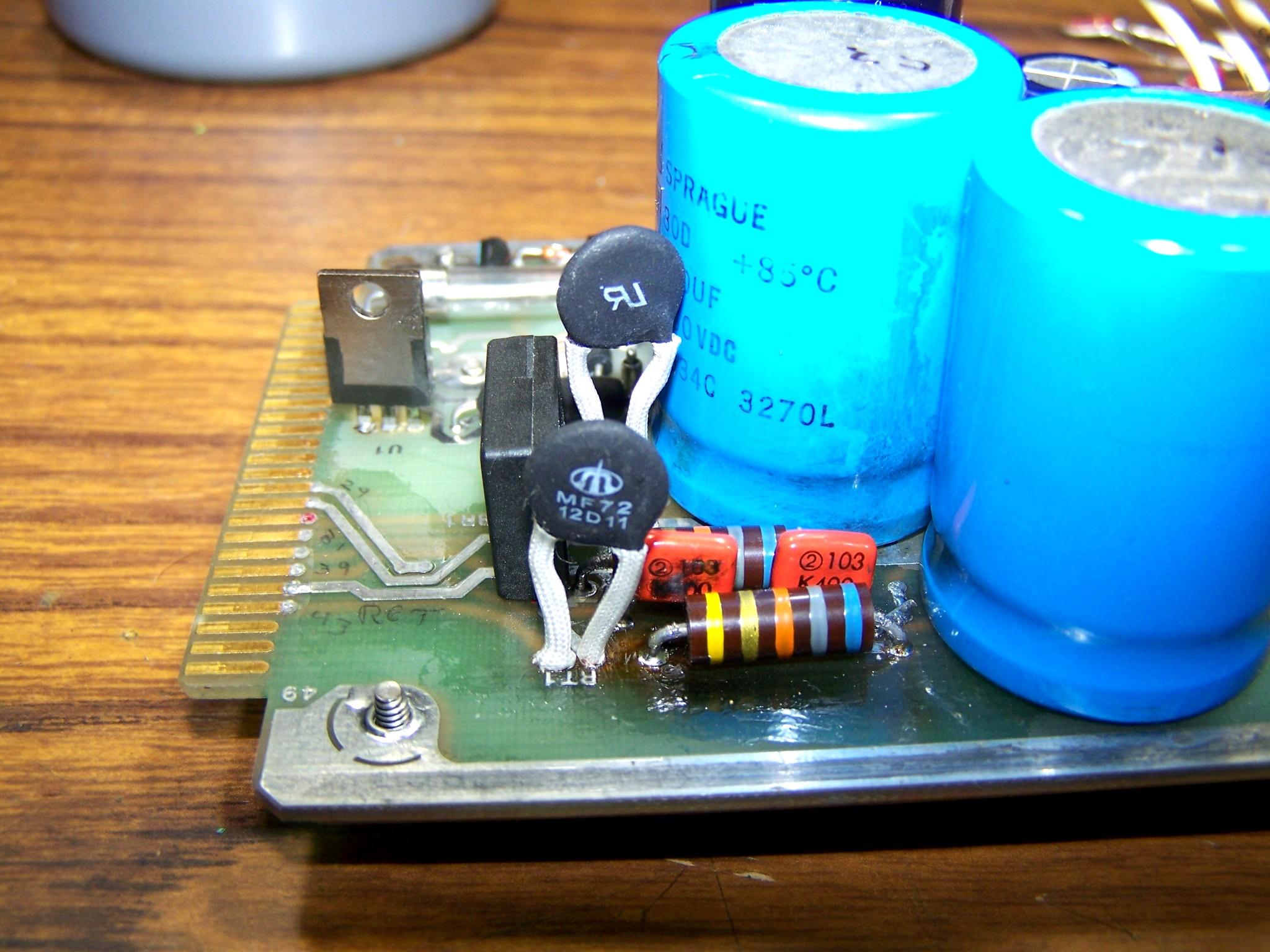
The thermistors used were suitable for the wide hole pattern and the leads were pre-bent for mounting. Straightening from the inside of the bend resulted in a perfect fit into the board. The leads were left long and fiberglass sleeves were used to keep the thermistors up off the board for adequate airflow, as they do heat up with time.
Failure Analysis:
So why did the thermistors on A3 fail? The most plausible reason any of us has guessed is that a high voltage AC line spike (possibly induced by lightning) caused the close traces to arc and the arc current eventually blew the thermistors.
Why wasn't more damage done? Dumb luck or Murphy's Law?
The 330VDC VC+ and VC- were alive and well. VC+ and VC- feeds the AC switcher board (A6) but as the unit was shut off, the switcher drive was not running and that is significant. With the drive off, everything down stream is fairly safe. The caps on both the A3 and A6 boards back-fed the arc and the dV/dT of the caps would have held the peak voltage down while RT1 and RT2 blew up, protecting the AC fuse.
Other D-Series Findings:
Unrelated to the power supply failure, I found that the A3 and A6 cards were a bit tough to pull the first time. A3 is attached to a metal heat sink that has two screws holding it (and the board) into the chassis. After applying grease to the edges and Nyogel to the card edge connector, they now go in and out quite easily.
I struggled a lot with A4 and finally got A5 out by alternatively pulling up on the white tabs and using a small flat blade between the card edge and the case to rock it slightly. Even after it was free from the socket it was HARD to pull out. Back to A4 with a little more room and the same rocking it came loose and it took a hand on top and the other on the bottom to pull it out.
Experience from removing other plug-in cards from two D-series units is that the cards are the maximum width to fit between the card guides. Along with lubing the guides and card sides, also lube the fiberglass card side edges. After this treatment the cards slide in and out easily. It goes without saying: use Nyogel on the card edge connectors.
Credits and Acknowledgements:
Circuit diagrams came from the Motorola R2001D Service Manual, 6881069A63 scanned by KB9MCI.
Thanks go to Bob WA1MIK for help locating suitable replacement thermistors, for taking a unit apart for photos and measurements, and for turning some notes into an article.
Contact Information:
The author can be contacted at: k7lzj [ at ] arrl [ dot ] net.
Back to the top of the page
Back to Moto Test Equipment
Back to Home
This web page created 07-May-2020
This web site, the information presented in and on its pages and in these modifications and conversions is © Copyrighted 1995 and (date of last update) by Kevin Custer W3KKC and multiple originating authors. All Rights Reserved, including that of paper and web publication elsewhere.