Up two levels (Moto index)
Back to Home
By Robert W. Meister WA1MIK

|
Up one level (GTX index) Up two levels (Moto index) Back to Home |
Taming the GTX 900 MHz Mobile Radio's Output Power By Robert W. Meister WA1MIK |
|
Background:
Many of us who use GTX 900 MHz radios to work amateur repeaters are well aware of the erratic output power problem. You go through the complete board replacement procedure, adjusting the deviation and output power, and everything looks great on the test frequencies of 896 through 902 MHz, and 935 through 941 MHz. After all, these are the bands that the radio was designed for and specified to work in. Then you program in and transmit on some amateur frequencies and you find various output power levels of 0.8 watts, 12 watts (where you aligned the radio's output power), or 19 watts. On one radio I have, I would get 12 watts on 902.4125 MHz and 902.4875 MHz (two repeater input frequencies), 19 watts on 927.6000 MHz (a simplex frequency), 0.8 watts on 927.5000 MHz (another simplex frequency) and 19 watts on 927.4125 MHz and 927.4875 MHz (two repeater output frequencies). Depending on the radio, the power remains controlled on some channels, while others are always erratic. Naturally, the radio still works just fine on the commercial frequencies it was designed for.
The GTX radios (as well as some other Motorola products) have 16 alignment points (sub-bands or frequencies) for power and deviation that are adjusted during board replacement or calibration procedures. In the case of the 900 MHz GTX mobile, there are eight of these points, in 1 MHz increments, at frequencies between 895.5 and 902.5 MHz, and between 934.5 and 941.5 MHz. When the radio transmits in these bands, the appropriate values for that frequency are pulled from the table and used to program the output power and deviation circuits. A problem occurs when an out-of-band frequency is used (902 - 935 MHz); the radio (or RSS) has no idea what value to use, because the sub-bands aren't calibrated for that frequency range. If it uses zero, the radio puts out 0.8 watts. If it uses a high value, the radio puts out 19 watts.
I have not yet figured out if the RSS determines the power and deviation values and sends that information to the radio during programming, or if the radio itself makes the determination of which values to use as the channel is changed. That's being saved for a future project.
Since the radio is incapable of controlling the output power properly when used in the amateur band, I've finally given in and decided to add a manual power control adjustment, so the output power is relatively constant across the frequencies of interest. There's a similar article about doing this to a MaxTrac on this page. The MaxTrac can also be modified to control deviation in the same way, by adding a pot. However the deviation in the GTX is controlled by the microprocessor which sends a digital value directly to the audio IC, rather than through external analog circuitry. So you can not add a pot to control deviation on the GTX radios.
I have tried using a "magic" code plug that, on some radios, seems to control the output power better, but even that has failed to produce consistent power levels, and on one radio it worked fine until I added a few more channels, then I was back to uncontrolled output power. I know I'm not alone in this experience; Dave N1OFJ has a radio with the same problem and he will be doing this modification very soon.
Another person also initially reported success with the "magic" code plug, but after he enabled scan on some channels, the output power reverted to its inconsistent behavior.
I recently repaired a GTX mobile radio that was displaying E06 all the time. I went through the entire board replacement procedure and the radio met all specifications. After programming it with amateur frequencies, including two scanning modes, the output power was either under 1 watt or over 15 watts, where it was previously making 12 watts. I removed the two modes from the scan list and disabled scanning, wrote the code plug back to the radio, and now it makes 12 watts on all amateur frequencies as well. Something big changes in the code plug when scanning is activated and it definitely affects the output power of the radio. Adding the manual power control is one way of straightening out this problem.
Please note that this article was written for the 12-watt 900 MHz GTX mobile radio. There is also a 30-watt version with a completely different circuit board but it has the same problem; most likely it uses the same firmware. The techniques and information presented herein may need to be adapted for other radios.
It is assumed that the reader knows how to remove the control head and cover from the radio and is familiar with soldering and working on delicate circuitry.
Circuit Analysis:
Refer to the schematic page below:
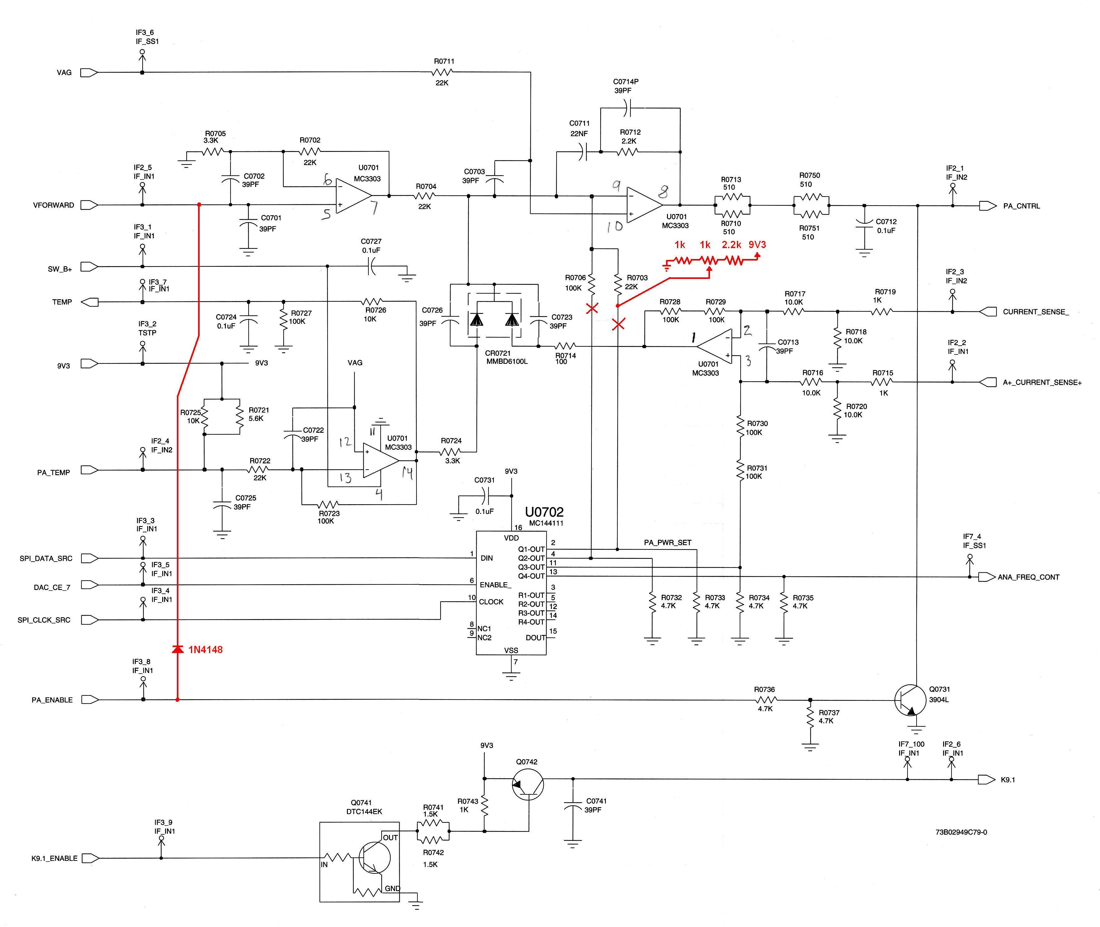
U0702 is a four-section six-bit Digital-to-Analog Converter (DAC). The output from pin 2 is the coarse power adjustment (labeled PA_PWR_SET), while the output from pin 4 is the fine power adjustment. These output voltages are controlled by the power settings done in RSS. These two signals go through R0703 and R0706 respectively, to U0701 pin 9, the summing junction for the power control circuit. This IC is underneath the main board of the radio. The adjustment value in RSS is an eight-bit number, so they use the top six bits to set pin 2 and the low two bits to set pin 4. Each of the 64 steps is about 14 millivolts.
U0701 is a four-section operational amplifier (op-amp). As is typical of all op-amps, when the voltage on the non-inverting input is higher than the voltage on the inverting input, the voltage on the output is high, and vice versa. This entire IC is devoted to power control in the GTX radio and it's easily accessible on top of the main board.
The power control circuit deals with four input signals:
These four signals are summed at pin 9 of U0701. The major players are the forward power voltage and the DAC control voltage. The temperature and current signals go through diodes (CR0721); this allows them to raise the voltage at pin 9, not lower it. Remember that an increase in the voltage at pin 9 (relative to the constant voltage on pin 10) will cause a corresponding decrease in the output voltage on pin 8 that controls the power amplifier. If the PA temperature or current gets too high, the output power will be reduced.
The power control circuit is a closed-loop system. The outputs from the DAC send a DC level through R0703 and R0706 to the summing junction, U0701 pin 9. For now, let's say the programmed voltage is 4.0VDC. This is compared to a reference signal on U0701 pin 10, which is nominally 4.57VDC. Since the non-inverting input voltage (4.57 at pin 10) is higher than the inverting input voltage (4.0 at pin 9), the output of U0701 pin 8 will go high. This tells the power amplifier to make more power. The forward power (actually voltage) is sensed and amplified through U0701 pins 5, 6, and 7, causing a positive voltage to be passed through R0704 to the summing junction. This voltage will now work against the signal already present at the inverting input of U0701 from the DAC, causing a rise in the voltage on U0701 pin 9. Eventually, the voltage at the inverting input will approach or even exceed the voltage at the non-inverting input, and the output of U0701 pin 8 will start to drop. As it does so, the output power of the radio will decrease, and this will lower the forward power sensed voltage. The entire system will come to equilibrium when the output power reaches a level specified by the DAC, as previously adjusted by settings in RSS. The voltage on U0701 pins 9 and 10 will be equal when the system is balanced and the output power is under control.
The above is a simplified and exaggerated description of the circuit operation. The voltage at the summing junction (U0701 pin 9) really only varies by microvolts as the power is adjusted, due to the balancing effect of the forward power sensed voltage through U0701 pins 5, 6, and 7.
What We're Starting With:
I connected the GTX 900 MHz radio to an Astron RS-12M power supply set to 14.00 VDC. The antenna connector ran through a 26-inch piece of RG58 cable to a 30dB, 50-watt attenuator. This was connected to an HP8901B Modulation Analyzer that can measure power up to one watt. The 30dB attenuator is convenient because it causes the analyzer to read watts as milliwatts. This is NOT a calibrated power measuring setup; it tends to read about 12% high at 900 MHz. I used a Fluke 189 digital multi-meter for the DC measurements.
Here's what we have to work with in the original circuit. The values are DC volts referenced to chassis ground at various power levels:
| Measurement Point | Rcv. | 0.8w | 9.6w | 12w | 19w |
|---|---|---|---|---|---|
| U0701 pin 8 | 0.2 | 1.11 | 3.20 | 3.33 | 11.96 |
| U0701 pin 9 | 8.4 | 4.57 | 4.57 | 4.57 | 4.08 |
| R0703 (U0702 end) | 8.5 | 8.42 | 4.35 | 3.97 | 0.72 |
| R0706 (U0702 end) | 8.5 | 1.28 | 1.00 | 1.00 | 1.28 |
The readings for 0.8 watts were obtained with the power control setting in RSS at 000, the lowest possible value, on a controlled frequency. The 9.6 watt readings were at the same power setting, but on a previously uncontrolled frequency.
One thing I did notice was that the control voltage (U0701 pin 8) varies considerably while the radio is transmitting, even though the output power is very stable (in those situations where it was being properly controlled). The voltage would rise almost 100 millivolts during the first 10 seconds of transmission. This is due to the control circuit maintaining the output power at the set value.
There are several things worth noting in the above table:
What We Need To Do:
Based on the information gathered above, we need to duplicate the existing conditions around the summing junction and U0701 when we modify the radio. We'll disconnect the two DAC outputs and substitute our own adjustment components, which will allow us to set the output power to some constant value regardless of the operating frequency and any DAC voltage set by RSS. This also means we will have to be satisfied with whatever power the radio generates on the other frequencies, after we've adjusted it on one specific channel.
The manual control voltage that replaces the DAC output must meet several conditions:
We can deal with these conditions as follows:
There are plenty of (nominally) 9VDC sources available in the radio. If we divide this voltage into nine equal parts, we need three volts as a minimum and a two volt range. This gives us 3, 2, and 4 volts to be dropped accordingly. A convenient ratio is 1000 ohms per volt. These translate to a 3k resistor to ground, a 2k pot, and a 4k resistor to +9.3VDC. We can use the nearest available standard resistor values. The schematic so far looks like this:
                      +---/\/\/\/--->(to U0701 pin 9)
                      |     22k
                      V-->
(GND)<---/\/\/\/---/\/\/\/---/\/\/\/--->(+9.3VDC)
           3k      2k pot      4k
This is fine except it doesn't deal with condition #1 above. If I could find a point in the radio that has +9VDC on receive and 0VDC on transmit, I could use that as the ground end of the above circuit. I did manage to locate just such a point, but it's underneath the board that we can't get to without removing the board; that's way too much trouble. Let's defer this problem until later.
Note that clockwise rotation of the pot I used moves the wiper arm towards +9.3 volts; this will cause the output power to be reduced. You could wire the pot the other way so a clockwise rotation goes towards ground and increases the output power.
Modifying the Radio:
CAUTION: The components in the GTX radios are extremely tiny. Use a very fine point soldering iron at about 25-40 watts. I found it easier to add a small bit of solder to the end of the wire, resistor, or diode lead, put the lead onto the point in the radio that I wanted to attach it to, then apply heat to the lead until the solder melts and the connection is made. This keeps the heat away from the easily damaged parts. If you aren't comfortable working on small stuff, seek the assistance of an expert.
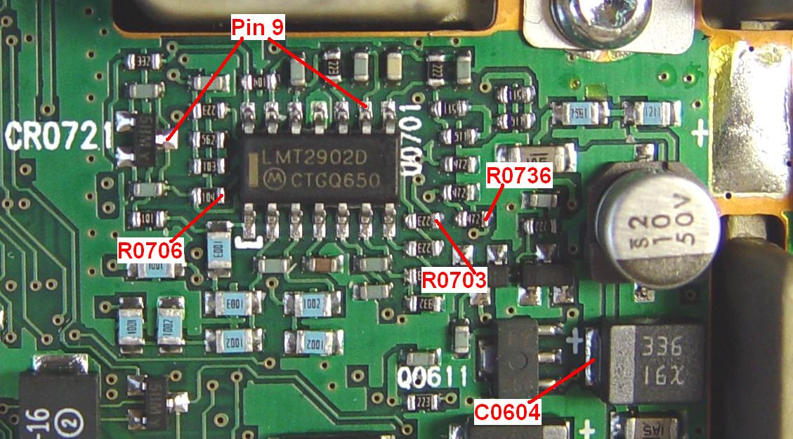
The photo below shows the component locations around U0701, which is located just below the lower left corner of the power amplifier shield (all references to left and right are with the radio on a table with the control panel towards you):
Here's the X-ray view of that area of the board:

First, we need to remove or disconnect R0703 and R0706 so the DAC doesn't control the output power any more. These are very small surface-mount resistors and I was unable to remove them non-destructively because the board has a conformal coating on it that holds everything in place.
I found it easier to make two small cuts, with a small knife, in the traces feeding these resistors. The trace from the feed-thru hole that goes to the right side of R0703 can be cut next to the feed-thru hole. The trace that goes to the right side of R0706 disappears under U0701 but can be cut right next to the left side of U0701. The photo below shows the two cuts on each side of U0701:
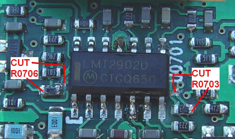
Both of these cuts are marked with a red "X" on the schematic, at the lower ends of R0703 and R0706.
Adding the Manual Power Control Circuitry:
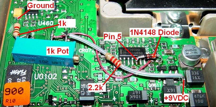
I found a nice source of +9.3VDC on the left side of C0604 which is conveniently located and directly at the output of the 9V regulator. Ground can be found on U0701 pin 11 or on several other large foil pads such as negative terminals of capacitors. I used the ground on C0460 because it was close. Use an ohm-meter to verify the ground point you choose. Key components are marked on the photo above.
If you look carefully at the first VDC value in the table below, you'll see that in receive it's sitting at 11.23 volts, not 0.2 volts as it was originally. Even though the radio is not transmitting, this violates condition #1 above. I deferred the solution until now.
I probed around near U0701 and found a convenient point on the right side of R0736 (PA_ENABLE) that has +4.9VDC on receive and +0.01VDC on transmit. I connected a 1N4148 diode (any small-signal silicon diode will work) from this point to U0701 pin 5. This causes U0701 pin 7 to sit at nearly 12 volts in receive, raising the summing junction voltage enough to shut down the power control voltage at U0701 pin 8, regardless of the voltage being supplied by the pot. The diode can have its leads cut very short and it can be soldered directly to the two connection points. Problem solved.
I bought a 1k, 15-turn pot, adjusted the component values, and tried this circuit, making use of R0703:
                      +---/\/\/\/--->(to U0701 pin 9)
                      |   22k (R0703)
                      V-->
(GND)<---/\/\/\/---/\/\/\/---/\/\/\/--->(+9.3VDC)
           1k      1k pot     2.2k

(to PA_ENABLE)<----->|----->(to U0701 pin 5)
                  1N4148
This reduces the component count to two fixed resistors, one potentiometer, and one diode. Their electrical placement is shown in red on the schematic above.
I used a drop of Super Glue to hold the 1k pot to the board, fairly close to U0701, but not covering anything important. Be careful when you choose your component locations as there are some protruding pieces of plastic inside the top cover that may cause interference.
The component leads were made as short as possible to connect to the components on the board. I used 30-gauge wire-wrap wire to the arm of the pot. I also used some 22-gauge plastic sleeving over the resistor leads to insulate them from the parts and the shield inside the top cover.
If you want to use your own 22k resistor, it can be connected from the arm of the pot directly to the right side of CR0711 (the summing junction) which is quite accessible. If you are going to re-use R0703 like I did, you may find it easier to attach the wire to the right side of that resistor before installing the diode over the top of it.
I connected the 1k resistor from the pot to the ground side of a nearby capacitor, C0460. I used a short piece of wire from the arm of the pot to the right side of R0703. The 2.2k resistor ran from the pot to the left side of C0604, the source of +9.3VDC. The diode was just soldered directly to U0701 pin 5 and the right side of R0736. Note that the banded (cathode) end of the diode goes (points) to U0701 pin 5.
Just about any single-turn, 1/4 or 3/8 inch square pot can be used if you can find a spot to secure it. You could even use a small piece of double-sided foam tape instead of gluing it down. Once you adjust it, you'll probably never have to touch it again. In fact, a suitable combination of fixed resistors could also be used, but I like the ability to set the power right where I want it, so I prefer to use a pot.
Final Adjustment:
After wiring up the circuit, set the pot to the end closest to the +9.3VDC supply (it will depend on the type of pot you use and how you orient the leads); this will produce the lowest output power. Connect a wattmeter and dummy load to the antenna jack, set the radio to a 927 MHz frequency, key the transmitter, and adjust the pot until you get 12 watts output. Change to a frequency in the 902 MHz range and measure the power there. You should see 12-14 watts.
Test Results:
After connecting the components shown above, I connected a DC voltmeter to U0701 pin 8, the power amplifier control voltage, to verify everything was working as expected. The table below shows the setting of the potentiometer, the output power, the control voltage, and the current draw of the radio for both circuit configurations.
| Power Pot Setting |
Without Diode | With Diode | ||||
|---|---|---|---|---|---|---|
| Watts | VDC | ADC | Watts | VDC | ADC | |
| Don't Care | RX (0) | 11.23 | 0.4 | RX (0) | 0.22 | 0.4 |
| Full CW | 7.80 | 2.79 | 3.5 | 7.80 | 2.79 | 3.5 |
| Middle | 10.60 | 3.25 | 4.1 | 10.60 | 3.25 | 4.1 |
| Somewhere | 12.00 | 3.84 | 4.5 | 12.00 | 3.84 | 4.5 |
| Full CCW | 15.00 | 4.75 | 4.9 | 15.00 | 4.75 | 4.9 |
The range is rather nice, and very easy to adjust even with a cheap pot. I see no reason to use a multi-turn pot, except perhaps for size, stability, and ease of mounting. The component values I calculated were close, but I didn't figure on all the interaction between the various sections of U0701. So much for design theory! Sometimes it's easier to just build it and play with the values until it works the way you want it to. If you want the maximum power to be a bit higher, change the 1k fixed resistor to 470 ohms.
I set the radio for 12.0 watts on 927.5000 MHz and measured the output power and control voltage (U0701 pin 8) on the other frequencies programmed into the radio:
| Freq. MHz | Watts | VDC |
|---|---|---|
| 902.4125 | 13.0 | 3.6 |
| 902.4875 | 13.0 | 3.6 |
| 927.4125 | 12.0 | 3.8 |
| 927.4875 | 12.0 | 3.8 |
| 927.5000 | 12.0 | 3.8 |
| 927.6000 | 12.0 | 3.8 |
The radio seems to put out a bit more power on the low end of the band compared to the high end of the band. Perhaps the circuit is a bit more efficient at the lower frequencies and the power amplifier generates a bit more power with a given control voltage. High-power 900 MHz GTX mobile radios are rated for 30 watts in the 896-902 MHz range, but only 20 watts in the 935-941 MHz range. Similarly, low-power units are rated for 12 watts transmit, but 10 watts talk-around. Many other Motorola radios are also de-rated at higher frequencies. I can live with consistent output power and only one watt of difference from end to end. Enjoy 900 MHz !
Acknowledgements and Credits:
Dave N1OFJ proofread the article and suggested some additional information.
Schematics and component layout information for the GTX radio were obtained from the Motorola GTX/GTX LTR/LCS 2000 Service Manual, 68P02948C85.
As always, lots of thanks go to Mike WA6ILQ of the Repeater-Builder staff, for hand-converting this article to HTML.
Contact Information:
The author can be contacted at: his-callsign [ at ] comcast [ dot ] net.
Back to the top of the page
Up one level (GTX index)
Up two levels (Moto index)
Back to Home
This article was originally posted in June 2006.
This web page, this web site, the information presented in and on its pages and in these modifications and conversions is © Copyrighted 1995 and (date of last update) by Kevin Custer W3KKC and multiple originating authors. All Rights Reserved, including that of paper and web publication elsewhere.