Back to Home
on the Motorola R2001B and R2001C
Communications Service Monitors
By Robert W. Meister WA1MIK

|
Back to Moto Test Equipment Back to Home |
Replace the Power Supply Capacitors on the Motorola R2001B and R2001C Communications Service Monitors By Robert W. Meister WA1MIK |
|
Background:
I acquired an R2001B for free because there was nothing visible on the display, and without it, these units are pretty much useless. A quick check revealed the CRT was completely disconnected. After plugging everything back in and splicing some wires, the unit powered up but the display text was extremely dim and I could see noise and saw-tooth squiggles running around the display; non-text scope traces were much brighter. Everything functioned though. Power supply filter capacitors were suspect.
After Steve K7LJZ did his analysis and repair work on his power supplies, I decided to tackle mine. Based on the date codes on the ICs, my R2001B was made in 1981-1982. The power supplies in the "B" unit are identical to those in the "C" unit. The full service manual for the "B" model can be found on this website. The Low-Voltage Power Supply section from my "C" manual (6881069A99-O) has been scanned to a 760 kB PDF file you can download here. I have amended and corrected the scanned pages. The High-Voltage Power Supply section has also been scanned to a 200 kB PDF file you can download here. The R2002 is an R2001 with the IEEE-488 (GP-IB) option. Other R200X models are still the basic R2001 with additional features, such as for trunking and cellular telephones. You'll have to create your own capacitor list and procedures for the "A" and "D" models, but they are probably similar.
I'll be referring to the R2001B as the Service Monitor (SM) from now on.
Repair Techniques and Helpful Tips:
These items apply to both power supplies and should help prevent you from getting into too much trouble.
Low-Voltage Power Supply (LVPS):
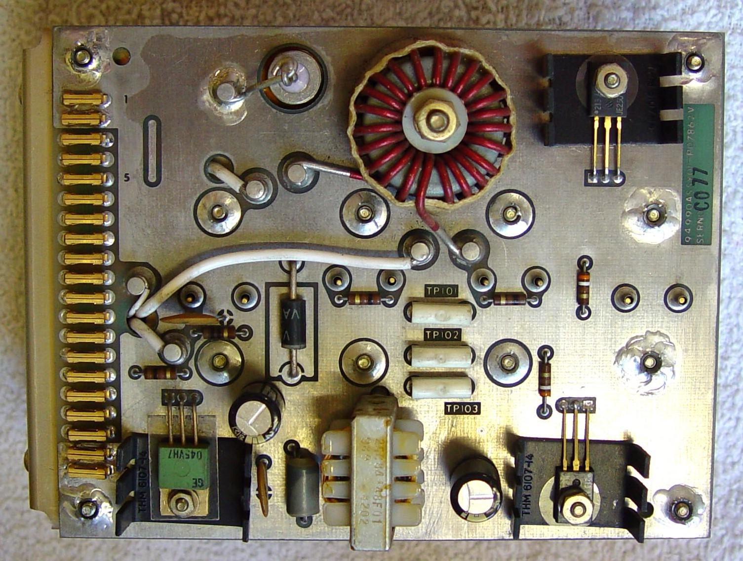
This assembly is covered in Section 6 of the manuals and is known as A1. It consists of four plug-in boards (A1A1, A1A2, A1A3, and A1A4), a motherboard, and a chassis. The LVPS is located at the rear of the SM. A 92mm 120VAC fan expels air out the back. The entire power supply assembly must be removed to do any repair work. While it was still in the SM, I measured the AC and DC voltages on the LVPS test points, located along the top edge of the boards. Based on the amount of noise and ripple (AC voltage), I decided to replace the electrolytic capacitors on all four boards. I did NOT replace the two large screw-terminal capacitors mounted to the A1 card because they're very expensive. I did have to remove them to gain access to the solder side of the A1 card.
The table below has the DC and AC voltage readings on the LVPS test points with the original capacitors as measured with a Fluke 189 DMM to TP201. The real DC test points should have minimal (under 10mV) AC voltage on them. Some test points have 20-40 kHz signals on them so they should have a significant amount of AC voltage present; these have (AC) in the "Signal Name" column. The first digit of the Test Point number represents the board it's on (1XX = A1A1, 2XX = A1A2, etc). The last two columns are the voltages after the capacitors have been replaced.
| TP | Original Caps | Signal | After New Caps | ||
|---|---|---|---|---|---|
| # | VDC | mVAC | Name | VDC | mVAC |
| 101 | 11.14 | 6,065 | Pulse Width Mod Out (AC) | 9.71 | 6,830 |
| 102 | 14.75 | 840 | Pulse Width Mod In (AC) | 13.12 | 800 |
| 103 | 14.47 | 848 | HV Source Voltage (AC) | 12.91 | 805 |
| 201 | 0.00 | 0 | Ground | 0.00 | 0 |
| 202 | 5.51 | 15 | +5V FB (or +5V?) | 5.21 | 13 |
| 203 | -5.28 | 19 | -5V | -4.99 | 3 |
| 204 | 13.67 | 17 | +12V | 13.15 | 10 |
| 205 | -13.99 | 20 | -12V | -13.16 | 3 |
| 206 | 35.33 | 147 | +33V | 34.13 | 8 |
| 207 | 123.11 | 25 | +110V | 117.21 | 21 |
| 208 | -123.11 | 30 | -110V | -117.23 | 16 |
| 301 | 7.93 | 12 | +8V | 7.93 | 36 |
| 302 | 15.09 | 605 | PWM Drive (AC) | 13.62 | 573 |
| 303 | 5.61 | 511 | Error Voltage | 4.92 | 277 |
| 304 | 12.83 | 28 | HV Bias Supply Voltage | 12.85 | 81 |
| 305 | 4.12 | 1,125 | Saw-tooth Voltage (AC) | 4.12 | 1,142 |
| 306 | 7.51 | 4,913 | Chopper Drive A (AC) | 5.25 | 4,540 |
| 307 | 7.51 | 4,903 | Chopper Drive B (AC) | 5.25 | 4,543 |
| 401 | 34.53 | 41 | Battery Charging Voltage | 0.00 | 60 |
| 402 | 14.55 | 615 | Freq Std Supply Voltage | 13.35 | 530 |
| 403 | 0.03 | 40 | Relay +12V | 0.00 | 113 |
| 404 | 15.13 | 625 | DC Bus Voltage | 13.97 | 532 |
Note that the +5V supply in my SM is 10% high and needs to be adjusted. This will affect all of the other DC voltages by the same percentage. Adjusting this means I will have to realign the unit afterward.
At 119 VAC, the unit draws 1.1 Amps and 128 Watts from the AC line.
Waveforms:
The following waveforms were taken with a Fluke 199C digital oscilloscope. Chassis ground was used as a reference. Only those test points with something worthwhile were sampled. The R2001B was in its default power-up state.
Test Point 101: Pulse Width Modulation Output
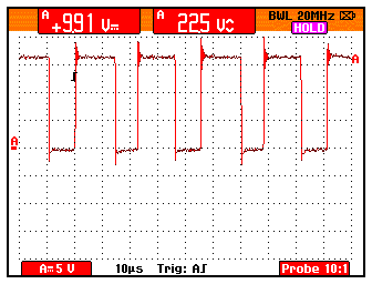
Test Point 102: Pulse Width Modulation Input
Test Point 103: High Voltage Source Voltage
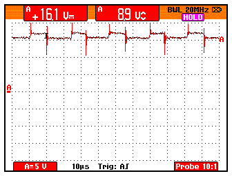
Test Point 302: PWM Drive
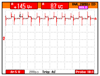
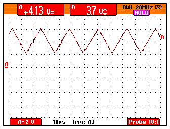
Test Point 305: Saw-tooth Voltage
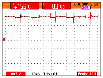
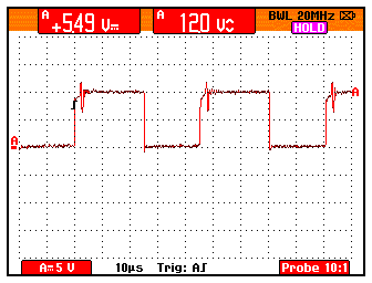
Test Point 306: Chopper Drive A
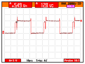
Test Point 307: Chopper Drive B
Removing the LVPS:
To remove the LVPS, remove both the top and bottom covers from the SM. Turn the SM on its right side. From the bottom, carefully unplug all three of the flat ribbon cables from the bottom of the LVPS assembly and unplug the cable that goes to the power transformer. Six screws, located around the fan on the rear panel, hold the LVPS in place. You do not have to remove the fan. Support the LVPS while you remove it, as it will fall towards the right side of the SM. With the supply sitting on the right side of the SM, slide it out from the bottom of the unit.
Note the orientation and location of the middle two cards (A2 and A3). They can be plugged in either way and they are NOT keyed, so you can also plug them into either slot, however the component size and placement on the other boards will prevent that from happening. Still, just do one board at a time. There are part reference numbers next to the ICs on A3, and A3 also has three pots along the top edge. The two end cards (A1 and A4) can't really be installed improperly because of their metal panels, but they could be swapped around. The panels are held in with flat-head screws on both sides of the card-cage as well as one or two pan head screws on the bottom. Mark their locations on the card-cage.
There are pictorial drawings in the manuals but it's easier to number the boards and put similar numbers on the card-cage along with orientation arrows so you know which way to plug them back in later. Incorrect installation will definitely release the lifetime supply of smoke and you're unlikely to find spare power supplies on ebay.
Replacing the LVPS Capacitors:
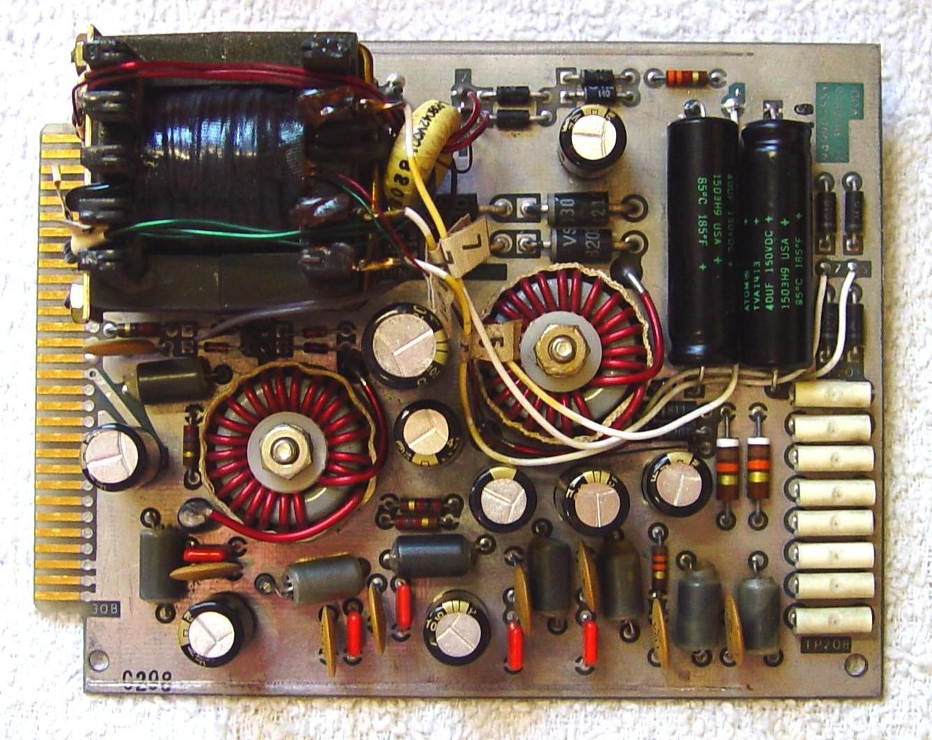
A1 Card:
You will have to take a lot apart to work on the A1 card, as the board itself is mounted on one side of a metal panel and transistors and a diode are installed through that panel. Remember to mark where the TO-3 components came from. Similarly identify the wires that go to the screw-terminal capacitors. The pictorial diagrams in the manual may not be entirely accurate or your unit may have had revisions done to it after the manual was printed. If they don't agree, put them back the way you found them, since it was obviously working before you took it apart.
The two large screw-terminal capacitors will need to be removed so you can gain access to the parts and board mounting screws behind them. Put indexing marks on the capacitors and mounting clamps so you can orient them properly when you put them back. Note carefully which wire goes to which capacitor; mark everything uniquely. The pictorial diagram shows two wires going to the shorter cap; if true, you might not need to mark the individual wires. It's better to mark them and not need those marks, than to omit marking them and then realize you needed to. I used a red "Sharpie" felt-tipped pen.
Initially I removed the screws from the caps, then removed the caps from their clamps, then removed the clamps from the mounting plate, which produced a lot of loose hardware. As I was reinstalling them, I found a much better way to deal with each cap:
Once these two big caps are removed, you can gain access to the hardware that holds the A1 card to the mounting plate. Note that one of the four TO-3 components (VR101) does NOT have plastic shoulder washers between the board and mounting plate, nor does it have a mylar insulator between the component and the mounting plate, as the case is grounded. This is the part that's furthest away from the screw-terminal capacitor mounting clamps. There is also a thin mylar insulator under the plate on the threaded end of the stud diode. I replaced the hardware on the stud diode after removing the board from the mounting plate.
Reassembly is the reverse of the removal process. With the board side of the mounting plate facing you, install the six shoulder washers into the appropriate holes in the mounting plate, then feed the wires through their holes and place the circuit board on top, squeeze the assembly together, flip it over, and install the board mounting screws until the shoulder washers are retained, then install the TO-3 components and tighten all hardware. The screw-terminal capacitors go back on at the very end. Here's a photo of the reworked A1 card. Click on it for a larger image.
A2 and A3 Cards:
Replacing the capacitors on the A2 and A3 cards is straightforward. I found that taking a photo, printing it out, and marking the positive end of each cap greatly reduced the chance of making a mistake. You can also make a mark on the circuit board, if you can find room to do so. I haven't seen polarity marks on any of the boards, but so far all of the positive terminals have had square solder pads on both sides of the board. Here's a photo of the reworked A2 card. Click on it for a larger image.
Here's a photo of the reworked A3 card. Click on it for a larger image.

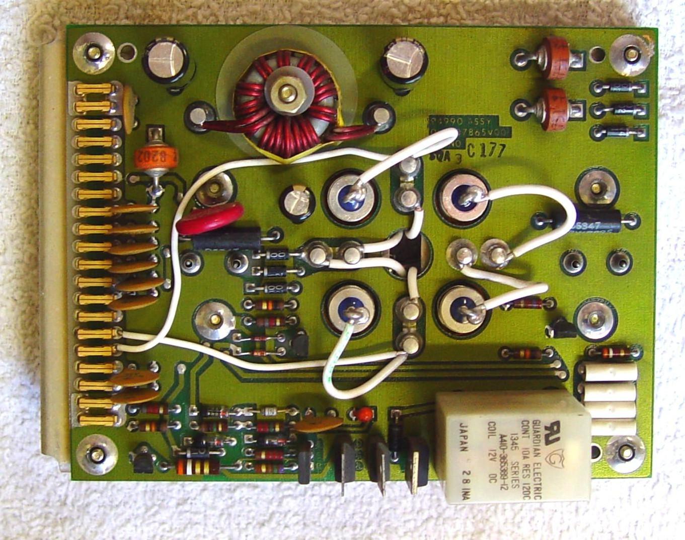
A4 Card:
You will have to take a lot apart to work on the A4 card, as the board itself is mounted on one side of a metal panel and transistors and diodes are installed through that panel. Remember to mark where the TO-3 components came from. Similarly identify the wires that go to the stud rectifiers. The pictorial diagrams in the manual may not be entirely accurate or your unit may have had revisions done to it after the manual was printed. If they don't agree, put them back the way you found them, since it was obviously working before you took it apart.
There are plastic shoulder washers between the mounting plate and the solder side of the circuit boards, to insulate the TO-3 component mounting screws. Don't lose these. Some may stick to the circuit board while others may stick to the mounting plate. There are also thin mylar insulators under the plate on the threaded ends of the stud diodes. There are lots of parts that can fall off and get lost. The wires that connect to the diode studs will fit through the slot in the mounting plate. Take extra care when disassembling the A4 card.
Reassembly can be a bit complicated. I placed the shoulder washers into the holes in the mounting plate, fed the diode wires through the slot, fed the diodes through their holes, making sure the insulators were still in place, and rested the circuit board on top. While squeezing it together, I flipped it over and installed the board mounting screws so they were snug but I could still move the board around. I then installed the TO-3 transistors and made sure everything lined up. Finally the diode hardware and wires went back on and I tightened up all the hardware. Here's a photo of the reworked A4 card. Click on it for a larger image.
Reinstallation of the LVPS into the SM is the reverse of the removal procedure. Slide the supply into the SM, lift it up a bit to start the screws through the rear panel, tighten the hardware, reconnect the three flat ribbon cables and the cable coming from the power transformer.
High-Voltage Power Supply (HVPS):
This assembly is covered in Section 16 of the manuals and is known as A10. The HVPS is located on the bottom of the SM, under the CRT, along the left rear side of the chassis. I was able to measure the 2nd anode voltage at 4,100 Volts using a Simpson 270 VOM on its 5,000 VDC range.
Removing the HVPS:
To remove the HVPS, remove both the top and bottom covers from the SM. From the top, disconnect the 2nd anode lead from the CRT (it snaps off), carefully unplug the CRT socket and protection board from the rear of the CRT, and unplug the five-pin, four-wire connector that goes from the protection board to the A2 card next to the CRT. Set the SM upright on its rear feet with the bottom facing you, and unplug the flat 8-pin ribbon cable from the side of the HVPS module. Loosen the two captive screws on the bottom surface of the HVPS. Gently pull the HVPS out of the chassis to unplug it from the card edge connector on the chassis above the HVPS. Thread the CRT socket, protection board, and cabling, as well as the 2nd anode lead down through the openings in the chassis as you remove the HVPS; these wires are all attached to the HVPS and they will get caught on just about everything on the back of the SM.
Replacing the HVPS Capacitors:
You will have to remove three metal-cased TO-3 transistors from the HVPS enclosure so you can remove the printed circuit board inside. Remember to mark where they go and how the hardware is arranged. I removed the six screws, the transistors, and their thin insulator sheets and set those aside. Notice that there are plastic insulators (shoulder washers) in the holes that the six transistor mounting screws came out of; you do NOT want to lose these. They must be positioned between the circuit board and the inside of the enclosure.
With the TO-3 surface of the enclosure still facing up, I then barely loosened the four screws in the corners that hold the printed circuit board into the enclosure, flipped the assembly over, and removed each screw with my fingers. The grommets around the wires come out through slots. I then lifted the circuit board up and out of the enclosure.
The reason I took it apart this way is that there are plastic shoulder washers between the inside of the enclosure and the back of the circuit board, that the transistor mounting screws pass through. When I first took it apart, I did NOT flip the assembly over and some of these washers fell out. I left them in the enclosure so I wouldn't lose them. Some may stick to the circuit board. If they do, remove them and place them in their appropriate holes inside the enclosure. The smaller diameter shoulder must fit through the enclosure. Make sure you put them into the larger diameter holes where the transistor mounting screws will pass through.
After you've replaced the three capacitors, insert the circuit board back into the enclosure, then thread the four mounting screws in from under the enclosure and up into the circuit board. Once they're finger-tight, flip the assembly over and verify that the six plastic shoulder washers are still properly positioned in the transistor mounting screw holes. Reinstall the transistors and their insulators using the six screws previously removed. Tighten all the screws when you're finished.
Reinstallation into the SM is the reverse of the removal process. Be careful when reconnecting the 5-pin connector on the A2 card, as it's hard to see. You may find it easier to partially slide the A2 card out of its slot to make reconnection easier.
Capacitor List:
The list below is sorted by board number (Bd) and capacitor reference number (C#). A1 through A4 are the LVPS; HV is the HVPS. Note that C21 in my HVPS was actually a 100uF / 50V cap rather than the 100uF / 35V cap as shown in the manuals. The capacitor list at the end reflects this difference; I bought a 50V cap. A higher voltage capacitor is always an acceptable replacement in electronic equipment.
Today's radial-lead electrolytic capacitors are much smaller than they were 30 years ago. I didn't bother looking for exact size matches or worry about lead spacing.
As I removed each capacitor, I measured its value. I've recorded these in the table below in the "Value" column so I could see what circuit was affected by the bad capacitors.
| Bd | C# | uF @ VDC | Notes | Value |
|---|---|---|---|---|
| A1 | 102 | 14,000 @ 30 | Screw Terminal; External; Not Replaced | 15,780 |
| A1 | 103 | 470 @ 25 | 590 | |
| A1 | 104 | 470 @ 25 | 641 | |
| A1 | 105 | 9,200 @ 15 | Screw Terminal; External; Not Replaced | 11,080 |
| A2 | 201 | 150 @ 50 | open | |
| A2 | 204 | 470 @ 25 | 514 | |
| A2 | 205 | 470 @ 25 | 509 | |
| A2 | 208 | 470 @ 25 | 501 | |
| A2 | 209 | 470 @ 25 | 531 | |
| A2 | 212 | 2,200 @ 16 | 2,531 | |
| A2 | 213 | 1,000 @ 16 | 1,240 | |
| A2 | 217 | 470 @ 25 | 482 | |
| A2 | 218 | 470 @ 25 | 514 | |
| A2 | 221 | 40 @ 150 | Axial Leads | 40 |
| A2 | 223 | 40 @ 150 | Axial Leads | 47 |
| A3 | 301 | 10 @ 25 | 12 | |
| A3 | 307 | 150 @ 50 | open | |
| A3 | 323 | 10 @ 50 | open | |
| A4 | 402 | 470 @ 35 | 624 | |
| A4 | 403 | 470 @ 35 | 612 | |
| A4 | 410 | 100 @ 35 | I used 100 @ 50 | open |
| HV | 15 | 47 @ 50 | 48 | |
| HV | 17 | 10 @ 25 | 12 | |
| HV | 21 | 100 @ 35 | Was 100 @ 50 in my HVPS | 98 |
The list below is sorted by the uF value. Digikey didn't have the axial-lead cap so I bought all the caps from Mouser. The axial caps are Vishay/Sprague and are the same part number as the board had originally; the rest are Panasonic radials. I tried to get all 105C-rated caps.
| # | uF @ VDC | Notes | Mouser Part Number |
|---|---|---|---|
| 2 | 10 @ 25 | 667-EEA-FC1E100B | |
| 1 | 10 @ 50 | 667-EEU-FC1H100LB | |
| 2 | 40 @ 150 | Axial | 75-TVA1413 |
| 1 | 47 @ 50 | 667-EEU-FC1H470B | |
| 2 | 100 @ 50 | 667-EEU-FM1H101 | |
| 2 | 150 @ 50 | 667-EEU-FM1H151 | |
| 8 | 470 @ 25 | 667-EEU-FM1E471 | |
| 2 | 470 @ 35 | 667-EEU-FM1V471 | |
| 1 | 1,000 @ 16 | 667-EEU-FM1C102 | |
| 1 | 2,200 @ 16 | 667-EEU-FM1C222 |
There are 22 leaded aluminum electrolytic capacitors that I replaced in the two power supplies. I did NOT purchase new screw-terminal capacitors for the LVPS.
Failure Analysis:
The open C410 (on A1A4) is possibly causing the excessive AC voltage on TP402 and TP404.
CR411 (on A1A4) has a much lower resistance reading than CR409, CR410, or CR412. I purchased a new MBR1530 and it too has a low resistance like CR411. The voltage drop across each diode with 1ADC flowing through them is not that much different. I might replace all four diodes eventually.
The open C323 (on A1A3) may or may not have affected the current limiting or voltage regulation.
The open C307 (on A1A3) was causing the "Batt" LED on the front panel to remain illuminated all the time, even though it was running on AC and I had no battery attached to my unit.
The open C201 (on A1A2) was causing excessive AC voltage on the +33V supply, as shown on TP206.
CR204 and CR207 (on A1A2) in the +5V supply had extremely low resistance readings and may or may not be defective. They're 5A 20V Schottky diodes that have a low resistance to begin with, but these were far lower than any other Schottky diodes I measured.
Power Supply Adjustments:
Apparently Motorola doesn't think technicians would know how to adjust the power supply pots, so there's no procedure in any of the manuals. There are three adjustments on the A3 card: Dead Time, Voltage, and Current Limit. The pots are labeled on the component side of the circuit board.
With the unit fully operational and set for normal power-up conditions, set the Dead Time pot fully CCW, then rotate it CW slowly while listening for a growling or groaning sound coming from the power supply. Stop when you hear that then rotate the pot about 10-15 degrees CCW. If you want to take the time to connect a pair of wires to Q103 and Q104's mounting screws, you can connect those wires to a dual-channel oscilloscope and adjust the Dead Time pot so the two square waves do not overlap at all. If they DO overlap, that means both transistors are turned on at the same time, and that load causes the power supply to growl or groan.
Use a digital multimeter set to a 5V range and connect it to TP202 on the A2 card and Ground to TP201. Adjust the Voltage pot on the A3 card for a reading of +5.2VDC. Check the -5VDC supply at TP203 and it should be -4.9VDC to -5.1VDC. If you DO adjust the voltage by more than 0.1V, you will most likely have to fully align the rest of the service monitor.
Turn the Current Limit pot CCW until the supply starts pulsing or shutting down, then back it off by 10-15 degrees CW.
The HVPS Voltage should be adjusted for -2,000VDC at the cathode of the CRT. This is hard to get to. I ended up pulling the tube socket off the back of the CRT and wrapped a small value resistor lead around pin 2 then put the socket back on, letting the resistor hang out the side where I could touch it with a probe. This gave me access to that pin and I used my 6kV high voltage probe to measure the voltage. Remove the resistor when you've finished. You can also measure the second anode voltage and set the high voltage to around 4,000 to 4,100 VDC but it's not as accurate.
Results:
I wish I could report instant success, but Murphy's Laws took effect.
I made sure the unit was turned off and plugged the power cord into the receptacle on the rear panel. About a second later there was a bright white flash from the fuse and it vaporized. I took a quick peek at the front panel and saw the "Batt" LED lit up, which is odd because there is no battery nor external DC power supply. But the fuse was toast. I later determined that some DC had been developed before the fuse blew, and the lack of AC caused the "Batt" LED to light up. So apparently it's normal for the "Batt" LED to light up briefly when the AC power from the outlet goes away.
I investigated the AC and DC power paths and determined that the unit might still work on DC power. I scanned a piece of the overall wiring diagram that shows the power input wiring; it can be found here as a 25kB PDF file.
I connected an external 14V 7A DC power supply to the unit; there's a very convenient junction buss inside the rear panel next to the DC fuse holder. In the STBY position the relay on the A1A4 card actuated and the unit powered up fine with external DC, so the problem is related to the power transformer, wiring, and four MBR1530 diodes on the A1A4 card, which I had been fiddling with earlier, in other words, the circuitry to the left of TP404 on the A1A4 card. While the unit was operating, it unfortunately didn't seem to have made any improvement in the display quality.
Then something else went wrong and the display became very bright, small, and blurry, and the external power supply went into current limiting. I had this problem previously when I first put the HVPS back into the unit but it resolved itself, or so I thought.
I pulled the LVPS and went directly to the A4 board. I found diode CR409's cathode (stud/case) was shorted to ground. I disassembled the mounting hardware, verified everything was present including the mylar insulator, and checked the diode by itself; it was fine. So I put all the hardware back on and the short was gone. I put the LVPS back into the unit, installed a new 1.5A 250V fuse, and carefully powered the unit up through my Variac. Everything worked like it should have and the unit was drawing about 1.1A. I did not leave it on long enough to see if the display was in its bad operating mode or not; I was just happy that it powered up properly and the "Batt" LED was NOT lit.
Now that the unit is running again, I adjusted the power supply for 5.2VDC on TP202 and measured the DC and AC voltages on the power supply test points. These have been recorded in the table at the top of this article. I observed what seems to be an excessive amount of AC on all the test points; this could be lead or meter placement and I will experiment to find a better ground connection than just the metal chassis.
I also measured the 2nd anode voltage at 3979VDC, however I need to readjust it since all of the other power supply voltages have changed.
Unfortunately the display is still as dim and blurry as it was before I started this, but the noise and saw-tooth squiggles that I saw on the display are completely gone. I now have to diagnose and repair the barely visible textual scope data on the CRT.
I subsequently decided to look into the dim text on the CRT problem, so I put the A2 (scope deflection) card on an extender. The CRT went back to its bright, blurry, tiny display mode. Taking the A2 card off the extender got it working again. This bothered me. I took voltage and resistance readings on the 10-pin cable going from the A2 card to the HVPS and something wasn't right. I measured 5.6 ohms to ground on the High Voltage Reference line, pin 10. This line goes to the high voltage regulator and adjustment pot and effectively turned the HVPS on as high as it could go. I pulled the HVPS and measured the same 5.6 ohms to ground at pin 10 of the printed circuit board connector. I took the HVPS apart, cleaned the connector and surrounding board areas, as well as the mylar insulator under the board, and the short went away. I now measured 53k ohms. I put the HVPS back into the unit and that took care of the bright, blurry, tiny display. I put the A2 card on an extender and it now works the way it does without the extender, so I can continue to troubleshoot the signals to find out why the CRT text is so dim while the CRT scope traces are nice and bright.
After chasing several signals, I decided to adjust the High Voltage. According to the "D" manual, there should be -2,000VDC on the CRT cathode; mine was -1,930VDC. So I increased it to -2,000VDC, which also increased the 2nd anode voltage from +3,980VDC to +4,110VDC. I had to readjust two pots on the A2 card as well as the Focus knob. The display is now MUCH brighter and clearer and very readable in room light. This doesn't seem like much but it's a 3.5% increase, which also boosts the filament voltage a similar percentage, from 6.2V to 6.4V, which increases the emission. I may push it up a bit higher.
Update August 2017:
After doing every possible test and measurement on the CRT, on the recommendation of Steve K7LJZ I purchased a Sencore CR70 CRT tester / rejuvenator for $50 and used the Universal Adapter that came with it. The CRT was listed in the setup book but it has an error: the G2 connection should be pin 7 (Accelerator grid), not pin 4 (Focus grid). There was no emission from the tube when I started, so I ran through every restoration and rejuvenation process a couple of times. When I finished, the emission test nearly pinned the meter. I put the CRT back into the SM and turned it on. Nothing. Nada. No display at all. Then I noticed the front panel Intensity control was turned fully CCW. I turned it to 1/3rd CW and was rewarded with a very nice bright clear display on the CRT. I touched up the Intensity Bias and Balance pots on the A2 card and will continue to go through the adjustment procedure, now that I can read all the screens. The CRT brightness increases quite nicely as the front panel control is rotated with no signs of blooming or distortion. It's as if a brand new tube was installed.
Also, the intermittent very bright / tiny display mode was eventually traced to a low resistance path (several ohms) to ground on the HV Sample line of the HVPS, possibly right at the card edge connector. This caused the HV regulator to think there wasn't enough high voltage and it boosted it as high as possible. Some cleaning of that area with a brass bristle brush cleared things up.
Test Equipment:
I used a Fluke 189 DMM for the AC and DC voltage measurements and for testing the Schottky diodes. I also used a Simpson 270 VOM for testing the diodes and initially measuring the CRT's 2nd anode voltage.
I used a Fluke 80K-6 high-voltage probe with my Fluke 189 DMM to measure the output of the HVPS at the 2nd anode connection on the CRT. A better measurement point would be the CRT cathode, which is supposed to be -2,000V, but it's not easily accessible.
I used a Peak ESR70 Capacitance and Equivalent Series Resistance (ESR) meter for measuring the old capacitors.
Acknowledgements and Credits:
This article was written as a follow-up to the one written by Steve K7LJZ, also available on this web site. We shared repair techniques and our experiences many times.
Schematic and pictorial diagrams came from the Motorola R2001C Service Manual, 6881069A99-O, which was given to me by Bernard Dier. Additional info came from the Motorola R2001B Service Manual, 6881069A93-O, available on this web site.
Contact Information:
The author can be contacted at: his-callsign [ at ] comcast [ dot ] net.
Back to the top of the page
Back to Moto Test Equipment
Back to Home
This article created 29-Apr-2016
This web site, the information presented in and on its pages and in these modifications and conversions is © Copyrighted 1995 and (date of last update) by Kevin Custer W3KKC and multiple originating authors. All Rights Reserved, including that of paper and web publication elsewhere.